Ensuring Quality and Reliability in Global Supply Chains
With the ever increasing rise of competition in the industry, the semiconductor manufacturing is moving towards highly specialized, advanced and complex processing of wafers. The supply chain is getting more global and fragmented where one node might be located in US, while the other in China, Taiwan or Malaysia with each node being managed by a different vendor. This multi-vendor policy helps the companies to get access to highly skilled individuals as well as highly specialized machinery that can deliver quality products in a cost-effective manner.
This model of having a specialized, fragmented supply chain can indeed provide certain benefits. It enables companies to innovate at a faster pace and expedite the product’s journey from the prototyping stage to the final packaged product. However, such a setup can present significant challenges for those tasked with monitoring operations and maintaining yield. For these individuals, navigating the complexities of this segmented supply chain can become a daunting task.
Addressing Lot Tracking Challenges in Product Testing Lifecycle
The predominant challenge lies in tracking lot splits across the product testing life-cycle, from the final product down to wafer and die levels. This difficulty primarily stems from differing naming conventions and data mapping practices employed by various vendors in the supply chain. The lack of ability to attribute failure to an individual die and track the node where the failure occurred greatly hampers the ability to find root cause of the issue.
Enhancing Supply Chain Management with yieldWerx Solution
Typically, the engineering team invests a significant amount of time in building relationships and consolidating data. This data is sourced from various nodes of the global supply chain, and its purpose is to track the processing of lots and wafers. However, this exhaustive task diverts the team’s attention from their primary role, which is to perform actual analysis. This becomes even more critical when it constitutes a compliance requirement to track individual die and wafer as mandated either by the customer or the industry.
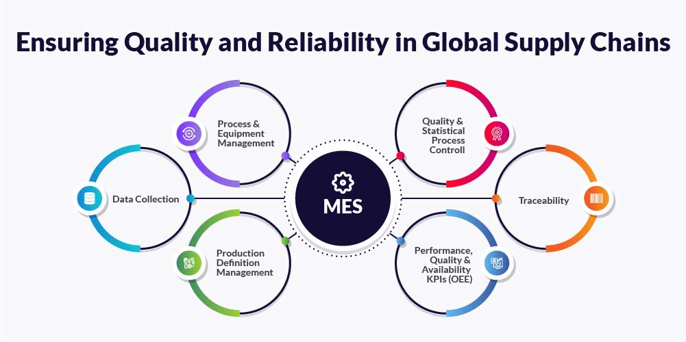
A powerful end-to-end yield management solution like yieldWerx lets the user automatically correlate data across multiple test points and nodes irrespective of the diversity and complexity of the supply chain through its powerful Lot Genealogy Module. The module is designed to streamline the management of extensive volumes of semiconductor manufacturing data. It swiftly associates data with various elements like vendors, equipment, lots, wafers, zones, and dies. This results in a cohesive and uniform view of the entire supply chain.
Efficient Lot Genealogy for Yield Maximization
Lot Genealogy in MES systems form the backbone of operational logistics, combining this data with ATE yield data is critical to resolving problems. The Lot Genealogy module facilitates data mapping and comparison across all manufacturing steps. This functionality empowers users to pinpoint a failing bin and review its performance at previous stages. This retrospective analysis occurs before the bin is officially marked as ‘failing’.
This module is quick and easy to setup and can track the lot genealogy with the help of simple clicks in real-time. The users can split a parent lot into multiple child and sub lots with everything intuitively mapped on a genealogy tree. The genealogy tree can then be used in yield and parametric reports and analysis to track lot splits, and the relationship to WAT/PCM, Wafer Sort and Final Test data.
Productivity Boost through Automated Lot Mapping
Effective implementation of Lot Genealogy information in yield management system is critical to solving business and operational problems. According to feedback from our customers, lot genealogy automation significantly boosts productivity, equivalent to the work of 5-6 full-time employees. Furthermore, it accelerates root cause analysis and leads to considerable yield improvements for semiconductor manufacturers.

