
In modern semiconductor manufacturing, raw test data is as valuable as silicon itself — but only when it can be properly organized and understood. Every wafer test, probe log, and final device measurement holds critical yield information buried under layers of unstructured noise. Without effective data manipulation, these insights remain hidden, leading to costly yield losses. That’s where an advanced yield management software (YMS) comes in. It automates the process of cleaning, aligning, and transforming massive datasets into actionable intelligence.
This blog post is your complete guide to understanding how semiconductor test data manipulation works, the challenges involved, and how integrated YMS platforms, like yieldWerx, streamline every step — from data ingestion and normalization to visualization and correlation.
What is Test Data Manipulation?
Test data manipulation in semiconductor manufacturing refers to the process of cleaning, transforming, and aligning raw test data so engineers can extract meaningful insights for yield optimization.
Some examples of Test Data Manipulation in Semiconductor Industry
Example 1:
Picture analyzing hundreds of wafer maps from different probe stations — each using its own coordinate system. Data manipulation aligns these maps, rotates axes, and merges datasets so engineers can identify a repeating edge defect pattern that would otherwise stay hidden.
Example 2:
A fab team merges wafer sort and final test results to trace a failing parameter back to a specific wafer zone. By manipulating and joining STDF datasets across test stages, they uncover a drift in a single etch chamber — preventing a full lot scrap.
Example 3:
Consider a lot where one tester logs a sudden spike in resistance readings. Through automated data manipulation, outlier detection filters out the noise caused by a faulty probe needle saving hours of false debugging and preventing incorrect process adjustments.
Industry Challenges for Data Manipulation in Semiconductor Manufacturing
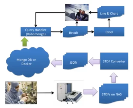
The chip testing process produces a massive volume of manufacturing data. To manage this continuous data flow, test systems transmit information through a gateway, which collects, formats, and outputs the results in STDF (Standard Test Data Format) or other standardized formats. These files are then sent to a central database or yield management system for further processing and analysis.
The goal of this system is to enable production managers and test engineers to quickly determine whether products meet quality standards and to identify performance deviations early in the process. However, achieving that goal requires overcoming several data infrastructure challenges that directly affect accuracy, speed, and scalability of semiconductor data manipulation. Some of them are:
1. Handling Massive Data Volumes
Every second, testers produce thousands of measurements per die — and there can be millions of dies per lot. This creates an overwhelming stream of data that must be received, stored, and processed efficiently.
A semiconductor test data management must achieve high throughput, meaning it should be capable of receiving and processing large amounts of data simultaneously without delays.
If the data flow is interrupted or too slow, engineers lose visibility into real-time production quality.
💬 Example: A fab testing 300 wafers a day can easily generate tens of gigabytes of STDF data every hour. Without a high-throughput system, file queues grow, slowing every step of analysis.
2. Slow Data Updates
Once tests are complete, the results need to be reflected in the system immediately. This requires low update latency, meaning the data management system must update results instantly so that the next process (such as packaging or binning) can begin without delay.
When updates are slow:
- Process engineers can’t react quickly to yield issues.
- The next stage of production (like assembly) may start before problem wafers are identified.
- Time-to-market is delayed.
💬 Think of it like waiting for a medical test result — you can’t start treatment until you know the outcome.
3. Data Ingestion and Storage Bottlenecks
In semiconductor testing, one of the heaviest tasks is ingesting raw test results into a database for analysis. This step can become a major bottleneck when:
- File formats are inconsistent.
- Network speeds are limited.
- Database systems aren’t optimized for large binary files like STDF.
A high-performance test data center must minimize insertion time — the time it takes to accept and write test data into the database. If insertion is slow, the data backlog increases, and real-time yield analysis becomes impossible.
4. Fragmentation Between Fabs, OSATs, and Design Houses
Fabless companies face a different challenge: data fragmentation. Their data comes from multiple foundries and test houses, each producing non-STDF data files in different layouts, using different bin codes and metadata.
Without automated tools, fabless teams must manually merge and clean this data, delaying insights and increasing the risk of human error.
5. Scalability and Infrastructure Maintenance
Legacy systems often can’t scale fast enough to handle the rising volume, especially when real-time processing or multi-site operations are involved.
Maintaining large databases, ensuring low latency, and managing global data synchronization becomes a major cost and resource challenge.
6. Security, Compliance, and Data Access
Both fabs and fabless companies handle sensitive design and production data, often under strict regulations such as ITAR, ISO 9001, or customer NDAs. Balancing accessibility for engineers with strong security controls (encryption, audit trails, role-based access) adds another layer of complexity to data management.
How to Manipulate Semiconductor Test Data for Yield Analysis
Manipulating semiconductor test data for yield analysis means transforming raw, tester-generated files into clean, structured, and analyzable formats that reveal performance trends, detect anomalies, and pinpoint root causes of yield loss. In modern fabs, this process combines automated data pipelines, NoSQL databases (MongoDB), and containerized cloud environments.
Step 1: Data Collection and Ingestion
Every semiconductor yield analysis begins with comprehensive data ingestion from multiple test stages such as wafer sort, final test, and reliability screening. Data typically arrives in STDF or ATDF, generated by Automatic Test Equipment (ATE).
Supplementary sources—like JSON logs, MES events, OPC-UA telemetry, and inspection images—add further context. Yield management platforms (YMS) like yieldWerx automate this process.
At this stage, engineers:
- Consolidate STDF and ATDF files from different testers, wafers, or lots.
- Merge data into a unified dataset for consistent downstream processing.
- Standardize naming conventions, parameter IDs, and measurement units across vendors.
Step 2: Parsing, Validation, and Cleaning
Once collected, data must be parsed into a structured schema and validated to ensure completeness and consistency. Missing fields, invalid values, or structural mismatches are corrected using yield management software before further processing.
The cleaning phase eliminates duplicates, fixes timestamps, normalizes units, and handles missing or corrupted entries. It also involves filtering out invalid tests due to equipment errors or operator interruptions. yieldWerx efficiently detects and discards statistical outliers using various techniques. You can learn more by reading the article below:
Ultimate Guide to Outlier Detection Using Part Average Testing
Step 3: Mapping, Categorization, and Enrichment
Next, engineers classify results into test bins that define pass/fail categories or specific defect modes:
- Bin 1 → Pass
- Bin 5 → Leakage Fail
- Bin 9 → Functional Fail
This binning enables the creation of wafer maps—visual grids that reveal spatial defect patterns like edge rings, center clusters, or random spot failures.
The enrichment process adds metadata such as lot IDs, part numbers, test head coordinates, and recipe versions, ensuring full traceability from wafer to device.
How YMS Helps:
- The software auto-generates wafer maps, showing pass/fail zones instantly.
- Highlights outliers and drift patterns visually.
- Engineers can spot defective patterns or systematic probe issues at a glance.
- Correlate parametric test data with optical inspection images.
Step 4: Normalization, Alignment, and Transformation
As STDF or non-STDF data comes from multiple testers and environmental conditions, normalization ensures that results are directly comparable.
Key normalization steps include:
- Unit standardization: Convert currents (µA/mA), voltages (V/mV), or frequencies (Hz/kHz) consistently.
- Environmental alignment: Adjust measurements for temperature and voltage variations.
- Coordinate transformation: Map tester die coordinates to fab floor positions or overlay inspection images.
Step 5: Statistical Correlation and Analysis
Normalized data becomes the foundation for deeper statistical correlation and yield modeling.
Common correlations include:
- Device-to-wafer correlation: Identifies electrical gradients across wafer positions.
- Wafer-to-lot correlation: Detects recipe drifts or equipment-induced shifts.
- Cross-stage correlation: Compares wafer sort with final test data to trace back failures.
These insights feed into SPC (Statistical Process Control) dashboards, machine learning models, or automated rule-based systems that continuously improve process yield.
Step 6: Storage of Semiconductor Test Data Using NoSQL Database
Cleaned and structured data is stored in a database layer that supports both performance and scalability.
While traditional relational databases follow ACID (Atomicity, Consistency, Isolation, Durability) rules for transaction reliability, they struggle with large, irregular semiconductor test data.
Instead, modern fabs adopt NoSQL databases like MongoDB, which operate on BASE (Basic Availability, Soft State, Eventual Consistency) principles.
MongoDB’s document-based storage makes it ideal for STDF-derived JSON data because:
- It’s schemaless, supporting diverse wafer and test formats.
- It allows horizontal scaling (adding more servers easily).
- It supports sharding to distribute massive test datasets efficiently.
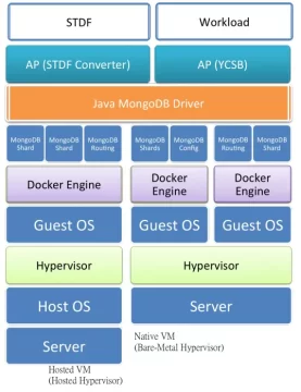
Step 7: Deployment with Docker and Containerization
For real-time test data environments, system reliability and fast recovery are critical. Traditionally, virtualization with full virtual machines (VMs) was used, but it required heavy hardware and long boot times.
Today, semiconductor testing systems leverage Docker containers:
- Containers share the Linux kernel, eliminating the need for separate guest operating systems.
- They start within seconds, reducing downtime.
- They consume fewer resources, increasing overall throughput.
In case of hardware failure, Docker enables rapid reconstruction of the execution environment, ensuring uninterrupted test data collection and analysis. These techniques keep the semiconductor test infrastructure secure, scalable, and high-performing.
Step 8: Continuous Monitoring and Quality Assurance
Finally, the end-to-end semiconductor data pipeline includes continuous monitoring of:
- Schema drift and data lineage.
- Record completeness and data accuracy.
- System uptime and container health.
By combining MongoDB with Docker modern semiconductor companies achieve a scalable, resilient, and automated data infrastructure for yield analysis — capable of handling millions of test records per day without downtime.
How YMS help here:
- Provides full data manipulation traceability across devices, users, regions and more. You can track every wafer, lot, and result.
- Stores secure audit logs and ensures data security compliance.
- Scales easily across test sites, fabs, and data formats.
- Built-in alert systems watch data live as it’s uploaded.
- When something looks off (like sudden yield drop or missing parameters), it sends instant alerts.
- Prevents bad data from going unnoticed or bad wafers from moving forward.
Test Data Manipulation Tools for Semiconductors
Several tools and platforms can be used to manage, manipulate, and analyze test data efficiently. The right tool depends on data volume, cost, integration needs, and automation goals.
1. In-House Scripts and Spreadsheets
Many engineering teams still rely on Python, MATLAB, or Excel-based scripts for data cleaning and visualization. These solutions are low-cost and highly customizable but demand continuous maintenance and technical expertise. However, they struggle with scalability when dealing with multi-gigabyte STDF datasets or when cross-lot comparisons are needed.
2. yieldWerx Platform
yieldWerx is a specialized, end-to-end yield data management and analytics solution designed for the semiconductor industry. It automates the full pipeline from data ingestion (STDF/non-STDF parsing) to yield visualization and reporting.
Key features & strengths include:
- Seamless integration with all the popular ATE outputs (STDF, ATDF, CSV, Klarf, etc).
- Automated data transformation, filtering, and normalization.
- Advanced correlation tools for wafer sort and final test data.
- Centralized storage enabling multi-user collaboration.
- Machine-learning modules for predictive yield analytics.
- Easy integration with PowerBI or JMP dashboards for executive decision-making.
With yieldWerx, a test engineering team can automatically merge wafer sort and final test datasets, detect systematic drift in under an hour, and share interactive reports across process teams — no manual scripting required.
Case Study: How Modern Yield Management Platforms Simplify Semiconductor Test Data Manipulation
A leading semiconductor manufacturer recently adopted yieldWerx to address challenges in consolidating complex final test data. Within just 4 weeks, yieldWerx’s engineering team deployed a cloud-based analytics environment capable of ingesting mixed, non-standard test files and converting them into structured, analyzable formats.
The solution used a configurable rules engine to automate regex validations, flag malformed entries, normalize wafer IDs, and standardize parameter formats. It also generated dynamic skip maps, allowing engineers to visualize probe coverage, prevent probe damage, and identify systemic yield issues in real time. Automated alerts highlighted data drift, bin mismatches, and missing parameters, while seamless integration with existing analytics tools enabled deeper statistical analysis and executive-level reporting.
Within a month, manual data reviews that once took days were reduced to hours. The platform delivered traceable yield insights, faster root-cause analysis, and measurable improvements in both yield recovery and time-to-market, demonstrating how an intelligent yield management software can transform fragmented test data into actionable, scalable semiconductor process intelligence.
You’ve just learned how data manipulation drives smarter semiconductor decisions. Now it’s time to put it into action. With an intelligent yield management system, you can go from scattered datasets to automated yield insights. Schedule a demo today and see what’s possible with yieldWerx.
Written by M. Rameez Arif, Content & Communication Specialist at yieldWerx.
Edited by Tina Shimizu, Content Strategist at yieldWerx.