Industries

Illuminating Data Analytics for Advanced & MicroLED and Image Sensor Products

yieldWerx is an end-to-end data and yield-analytics platform purpose-built to manage extreme-scale semiconductor data with full lifecycle traceability. The platform ingests electrical and optical wafer acceptance data, pixel-level parametrics, coupon die measurements, ASIC parameters, assembly & module results, and final test outcomes.

yieldWerx enables combined analysis of ASIC + LED + image-sensor devices, including bonded wafers, in a single environment—delivering true system-level intelligence from discrete wafers to final modules.

Photonics & LED Manufacturing
Navigating the Complexities of the Advanced and MicroLED Industry:

The challenge is no longer collecting data — it is turning it into trusted intelligence that feeds AI, design, manufacturing, and field performance analytics. AI models rely on clean, trusted, high-granularity manufacturing data to unlock performance advantages such as:

  • Ultra-high brightness and uniformity
  • Ultra-low defectivity at the pixel level
  • Accurate depth, ranging, and gesture detection
  • Lower power consumption and thermal stability
  • Higher reliability for consumer environments
Photonics & LED Manufacturing 01

Key Challenges

Managing Extremes

Managing ultra-high brightness and uniformity mixed with ultra-low defectivity at the pixel level. Maintaining brightness, sensitivity, and accuracy over long operating lifetimes and varying consumer environments.

Micro-Level Accuracy

Detecting depth, range, and gesture with absolute precision

Thermal Power Consumption

As devices become smaller and more densely integrated, managing heat while minimizing power draw becomes increasingly critical
How It Works

Modules that address key challenges

Comprehensive Quantitative Analysis

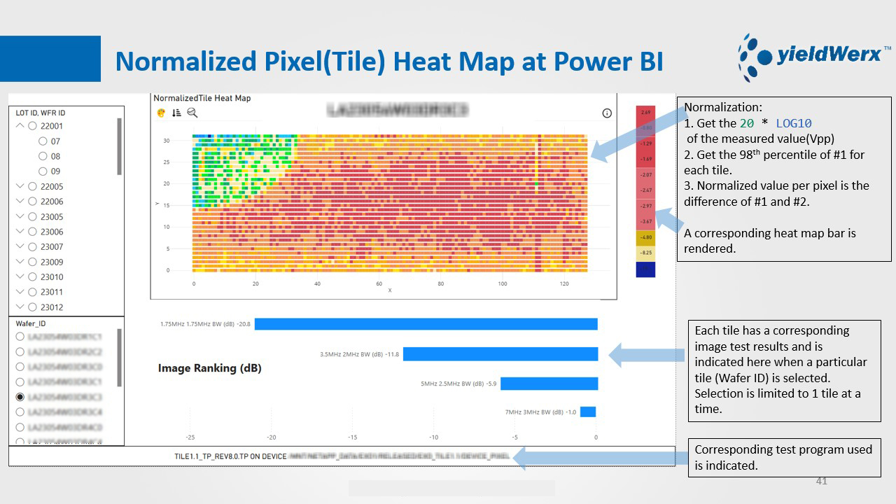
Analyze millions of die and billions of pixel-level measurements for color, brightness, and spectral performance; supports PAT, PCA, and DOE-ready datasets to turn complex MicroLED data into actionable insights.

Robust Statistical Process Control

Continuous monitoring of pixel, electrical, and optical test data across production runs; supports GDBN/GDBN-Z workflows, early deviation detection, and root cause analysis to maximize yield stability.

Defect Management

Advanced pattern recognition, defect clustering, and anomaly detection at the pixel, die, and module levels; includes auto pick-map generation and correlation with inspection and metrology data.

Integrated Systems Support

Supports complex assemblies like MicroLED displays, high-power LED arrays, and hybrid photonic-electronic modules, ensuring seamless multi-stage analysis.

Unified Data Repository

Harmonizes electrical, optical, assembly, and defect inspection data across wafer probe, OWAT/EWAT, module assembly, burn-in, and final system test for cross-stage analytics.

Process & Yield Analytics

Provides end-to-end visualizations and supports DOE, PCA, ANOVA, T-Tests, and parametric analyses across massive datasets to accelerate yield ramp and device optimization.

Automated Analysis & Dispositioning

Merges wafers/modules across multi-insertion runs and diverse datasets using custom rules, reducing manual effort and maintaining consistency.

Quality Control & Risk Containment

Outlier detection with predictive analytics and virtual binning using custom optical/electrical limits for early defect identification and yield preservation.

AI-Powered Commonality & Root Cause Analysis

Leverages AI/ML-driven knowledge graphs and cross-center analytics to pinpoint yield loss sources across lots, sites, and production stages.

Auto Lot Disposition

Compares cross-lot performance to detect inconsistencies caused by materials, process variations, or environmental factors; supports actionable disposition decisions.

Scalability Across Product Types

Tracks parameters and yield metrics across multiple MicroLED device types, including 2.5D/3D-packaged and hybrid assemblies, without sacrificing performance.

End-to-End Lifecycle Traceability

Maintains complete genealogy from Fab → Wafer → Module → Final Device, enabling backward/forward trace, RMA investigation, and process correlation across the full manufacturing flow.

Sharpen Your Competitive Edge

Discover the yieldWerx difference and revolutionize your semiconductor operations. Schedule a demo today!

Success Popup Widget
PTC-Logo

PTC

Partner

PTC is a semiconductor consulting firm based in Malaysia, providing strategic and technical consulting services to semiconductor manufacturing, assembly, test, product and ecosystem companies across Asia. yieldWerx, a leading innovator in semiconductor yield management solutions, and PTC, a premier Malaysia-based consulting firm for the semiconductor manufacturing industry, have announced a strategic collaboration to address the growing need for comprehensive data analytics across the semiconductor manufacturing lifecycle in the rapidly expanding markets of Malaysia and India.
This collaboration combines yieldWerx’s state-of-the-art analytics platform with PTC’s extensive industry knowledge and regional presence to strengthen semiconductor manufacturing capabilities across East Asia. By providing sophisticated analytics solutions tailored to regional needs, yieldWerx and PTC aim to streamline factory setup and operations, implement rigorous quality assurance protocols, and accelerate the development of sustainable semiconductor ecosystems across both countries. PTC will act as the regional consulting partner, offering advisory, deployment support, and strategic integration services to fabless clients, OSAT facilities, and manufacturing startups adopting the platform.