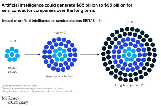
An estimated $5–8 billion in Semiconductor earnings are attributed to AI/ML initiatives across device makers, driven by streamlined operations, workflow optimization, and AI’s predictive capabilities to reduce waste. Independent analysis by McKinsey shows this could rise to roughly $35–40 billion. The increase does not come from entirely new use cases, but from compounding effects as AI is scaled across tools, fabs, and product portfolios. These gains are not driven by futuristic promises or isolated pilot projects; they result from concrete improvements in yield, throughput, equipment uptime, quality control, and working capital efficiency. In an industry where a single percentage point of yield can translate into millions of dollars, AI changes the economics by accelerating decisions, revealing hidden process relationships, and reducing the time between signal and corrective action.
This article examines where AI and ML are delivering real cost savings in semiconductor manufacturing today, how those savings compound across the fab and the broader value chain, and why scaling remains elusive for many organizations. It also looks ahead to what the next four years are likely to bring as AI becomes a foundational force multiplier for yield, productivity, and profitability across the industry.
How Much Can Semiconductor Companies Save Using AI/ML?
According to McKinsey, AI-driven analytics is reshaping the economics of semiconductor manufacturing by reducing lead times by as much as 30 percent, improving production efficiency by around 10 percent, and lowering capital expenditure by roughly 5 percent through more intelligent process optimization.
In practical terms, a single product example makes the arithmetic obvious:
Improving wafer yield from 93% to 98% at a foundry cost of $6,000 per wafer and 200 wafers per month saves about $60,000 per month or $720,000 per year for that one product alone.
Multiply that effect across tens or hundreds of products and across dozens of fab lines and the industry totals quickly align with the cited estimates.
Yield risk also increases significantly at advanced nodes. Modern 7nm, 5nm, and 3nm processes can involve 500 to 1,000 individual process steps, with each step introducing potential defect sources. A contamination issue introduced early in the flow may remain undetected until much later, by which point large volumes of wafers may already be affected. As process complexity rises, traditional yield management approaches struggle to match the speed, scale, and variability of today’s semiconductor manufacturing environments.
At the factory level AI/ML delivers value by accelerating decision velocity, extracting signal from terabytes-per-day process streams, and converting marginal percentage improvements into large dollar returns because fabs run at massive scale and razor-thin tolerances.
What Are the Core Areas Where AI/ML Reduces Costs and How do Savings Compound?
Manufacturing Efficiency and Yield Uplift
Manufacturing is where most absolute dollars are won. Machine learning enables per-wafer and per-batch process adjustments, virtual metrology that reduces physical sampling, and real-time fault detection that prevents excursions before they cascade into scrap. Together these interventions reduce cost of goods sold and increase throughput.
Typical concrete outcomes include cycle-time variability reductions on the order of 20–30 percent, reductions in physical metrology sampling of roughly 50–60 percent, and yield lifts of a few percentage points. Because fabs produce millions of die per month, those single-point yield improvements map directly to millions of dollars in avoided cost and incremental revenue.
Predictive maintenance and uptime
Unplanned downtime is extremely costly in modern fabs. ML-based predictive maintenance analyzes multi-parameter sensor streams to identify precursor signals hours before failure. Proven implementations reduce unplanned downtime by 10-20 percent and cut maintenance planning time by roughly half. That combination reduces both direct maintenance spend and the opportunity cost of lost production time, translating to multi-million-dollar annual savings per high-volume line.
Quality, defect detection and scrap avoidance
Computer-vision models and hybrid physics–ML detectors convert manual wafer inspection into continuous, automated systems that catch subtle defects earlier and reduce false positives. Industry deployments report dramatic reductions in escape rates and overkill, lower scrap, and fewer customer returns. The economics are straightforward: less scrap, fewer retests, and shorter debug cycles all lower cost per good die and reduce customer-facing warranty and service penalties.
R&D and design productivity
AI in electronic design automation and verification compresses design cycles, reduces iterations, and accelerates verification. Generative design and surrogate simulation models let teams explore orders of magnitude more architecture and layout variants, reducing design time and tape-out risk. Savings here show up as lower R&D spend per product, faster time-to-market (which preserves higher margins), and reduced NPI rework costs—effects that compound across a company’s product portfolio.
Inventory, working capital and supply-chain resilience
Demand forecasting and risk-calibrated inventory optimization lower the amount of safety stock required while preserving service levels. AI forecasts reduce forecast bias and improve fill rates; risk models identify where to hold buffer inventory most efficiently. Across the supply chain these advances can cut inventory and obsolescence materially, freeing cash and reducing total landed cost.
Energy and infrastructure efficiency
As node complexity and compute needs grow, energy is a nontrivial line item. AI helps optimize tool setpoints, rack densities, cooling regimes, and job scheduling to reduce energy per computing or processing unit. At scale, these savings reduce operating expenses and extend the life and density of existing facilities before incremental capex is required. TSMC reduces peak power consumption of EUV tools by 44% to save 190 million kilowatt-hours of electricity by 2030.
Why Semiconductor Companies Struggle to Scale AI/ML?
There are five recurring reasons pilots fail to scale into material financial outcomes.
Data Friction
Heterogeneous tool stacks, inconsistent wafer traceability, siloed and unclean data make it painfully expensive to assemble the labeled, clean datasets that production-grade models require.
Skills and Cultural Gap
Domain knowledge must be encoded into models and interpretation layers; process engineers must trust and understand model behavior. Without domain-led model pipelines and visualization that translates outputs into engineering actions, adoption stalls.
MLOps
Training a model in a lab is only the opening act. Production requires versioned deployments, drift detection, automated retraining, rollback capability, and cross-product transferability. Many fabs lack a reliable ML Ops practice, so models never reach sustained production.
Governance & IP Posture
Data governance worries about sharing sensitive process data or exposing procedural IP blocks are a big hurdle. They often prevent cross-site learning and partner collaborations that would otherwise improve model robustness.
Human Trade-Off Problem
Models suggest multi-objective optimizations—trade yield against energy, chemical consumption, and throughput. Only human engineers can define those trade-offs and the organizational KPIs that resolve them. If a company treats AI as a black box that “optimizes” without engineering oversight, it will optimize the wrong economics.
The Next Four Years — A Pragmatic, Scenario-based Outlook
Over the next four years, the semiconductor AI landscape will be shaped by two converging forces:
- The spread of foundational capabilities such as data platforms, MLOps, and edge inference
- The concentration of value among early adopters.
Companies that scale these capabilities across fabs will secure most of the initial savings within the first two years and, by year four, convert those gains into durable operational and margin advantages. Investment in strong data infrastructure, cross-fab learning, and production-grade MLOps will translate into measurable improvements in yield, cycle time, and capital efficiency, while firms that remain in pilot mode will struggle to move beyond isolated successes.
Deloitte’s latest State of AI Report indicates that AI maturity is rapidly becoming a defining competitive factor, shaping margins, speed to market, and resilience to supply chain volatility.
As the decade progresses, AI is expected to transition from an experimental capability to a standard operational backbone across semiconductor design, manufacturing, and planning, reinforcing a widening performance gap between leaders and late adopters.
What High-performers Do Differently?
Leading fabs treat AI as an operating-model change rather than a project. They create centralized centers of excellence that include process engineers, ML engineers, and domain data scientists. They embed models directly into operator workflows and hold AI programs accountable to 2–3 business KPIs (for example, yield delta, throughput, and unplanned downtime).
Here’s how you can also implement best practices for AI in semiconductor manufacturing:
1) Start With Process-critical Pilots
Begin AI deployment in high-impact steps such as lithography, etch, or deposition, where small process variations can drive major yield losses. Focus on a single tool or chamber and target use cases like predictive maintenance, virtual metrology, or defect detection. Validating performance and ROI at this level enables safer and faster scaling across the fab.
Read our Complete Guide to Defect Detection Using Knowledge Graphs.
2) Establish a Unified Data Foundation Before Scaling
AI performance depends on clean, connected, and contextualized manufacturing data. Semiconductor manufacturing processes generate massive volumes of tool telemetry, inspection results, metrology data, and MES records, but these datasets are often fragmented across systems.
Standardizing data pipelines, ensuring data quality, and enabling cross-tool visibility allows AI models to identify true process drivers rather than isolated correlations.
A strong data foundation also enables faster deployment of new models, consistent performance across tools, and long-term scalability as process complexity grows.
3) Build Yield-driven Workflows
Yield loss often results from small deviations accumulating across multiple process steps. Connect wafer inspection data, inline metrology, and equipment behavior across the production flow to identify hidden correlations and predict downstream failures. Integrated, real-time AI workflows enable earlier interventions, faster root-cause detection, and sustained yield ramp.
Read our article on Overcoming Semiconductor Yield Management Challenges Using AI and ML
Conclusion
The arithmetic is simple and unforgiving: small percentage improvements at wafer scale become large dollar outcomes. AI and machine learning act as a force multiplier that converts engineering insight into sustained margin growth, but only when companies invest in clean data, strong ML operations, workflow integration, and domain-driven model design.
The industry estimates of $5–8 billion per year today and roughly $35 billion over the next few years are not hypothetical; they are the sum of millions of discrete, implementable gains across manufacturing, maintenance, quality, R&D, and supply chain.
If your organization is still running AI as a set of pilots, the immediate priorities are clear:
- Fix wafer-level traceability
- Pick 7–10 high-impact use cases tied to business KPIs,
- Build ML Ops discipline
- Make process engineers the owners of model outcomes.
Those moves convert statistical gains into finance-grade returns.
To move from pilot to material margin, consider solutions that embed AI into yield workflows and give engineers the tools to act on insights.
If you want help turning wafer-level data into predictable yield improvement and measurable cost reductions, explore proven yield-optimization platforms such as yieldWerx that are designed to connect AI insights directly to engineering decisions and financial outcomes.
The numbers are real, the mechanisms are well understood, and the time to act is now: deploy AI not as an experiment, but as a core capability that multiplies yield and unlocks sustained profit.
Solutions like yieldWerx enable smart manufacturing to overcome AI scaling challenges. Schedule a free consultation with our experts to identify the hidden potential in your manufacturing workflow.
Written by M. Rameez Arif, Content & Communication Specialist at yieldWerx.
Edited by Tina Shimizu, Content Strategist at yieldWerx.
List of References:
- Mckinsey, Silicon squeeze: AI’s impact on the semiconductor industry
- McKinsey, Scaling AI in the sector that enables it: Lessons for semiconductor-device makers
- Generative AI for Semiconductor Design and Verification
- Fabs Begin Ramping Up Machine Learning
- AI-Powered AOI in Semiconductor Manufacturing: How to Upgrade Your Fab from Legacy Inspection Tools to Smart Yield Control
- AI And Competitive Advantage In The Agentic Era
FAQs
What is ML Ops?
MLOps (Machine Learning Operations) is the discipline of building, deploying, monitoring, and maintaining machine learning models in production reliably and at scale. Think of it as DevOps for AI/ML.
What is Virtual Metrology?
Virtual metrology for yield optimization uses process data to predict measurement results without relying solely on physical inspection. Models trained on historical production data estimate film thickness, critical dimensions, and other key parameters from equipment sensor readings.
This approach can cut metrology steps by 50 to 70 percent while maintaining quality standards, reducing inspection costs and speeding up production across the fab.
What is NPI rework cost?
New Product Introduction (NPI) rework costs refer to the expenses incurred when changes, corrections, or redesigns are required during the transition of a product from the design phase to full-scale manufacturing.
What is Edge Computing?
Edge computing is a way of processing data close to where it’s generated, instead of sending everything to a distant cloud or data center.
What is McKinsey?
McKinsey & Company (usually called McKinsey) is one of the world’s most influential management consulting firms. It advises governments, Fortune 500 companies, tech firms, banks, and manufacturers on strategy, operations, cost, and transformation.