Assembly Map Generation

Assembly Map Generation Featured Image
Ink/Inkless Wafer and Reticle Mapping

Optimize wafer test efficiency with full control and seamless integration between prober and wafer test sites, enabling testing, inking functions, and the identification of unique probing sequences for wafer and reticle sites. Equipped with AMG capabilities, Package and Board Management features, as well as Wafer bank grading. 

Submodules

Assembly Map Generation (AMG) 

Automatically generate Inkless Assembly Maps, also known as Ink Maps, for instances where physical inking may be necessary, merging Assembly Maps with additional data to enhance assembly maps.  

Advanced Packaging and Board Management 

Analysis of Serialized System and Board data, ensuring traceability from the System and Board level to the Packaged Die and throughout the entire product lifecycle.  

Wafer Banks, Screening & Grading 

Enables manual scrap or downgrade die, as well as selectively picking dies from wafers, enabling tracking to specific assembly lots rather than selecting an entire wafer. This capability is particularly beneficial for low-volume applications in the Aerospace and Defense sectors.  

How Can This Module Benefit You?

Ink and Inkless Wafer and Reticle Mapping 

Automatically generate inkless assembly maps between prober and wafer test sites 

Advanced Packaging and Board Management​

Collection and analysis of serialized system and board data for traceability to packaged die across product lifecycle 

Controlled Wafer Banks, Screening & Grading 

Allows manual scrap or downgrade of die as well as pick die from wafer rather than complete wafer 

Enhanced Decision-Making 

Facilitates informed data-driven decisions to ensure timely intervention 

Root Cause Identification 

Supports comprehensive root cause analysis and failure correlation from different test phases

Unified Data Analysis

Combines test results from wafers, packaged die, and system boards for holistic view 

Assembly Map Generatio (AMG)

Assembly Map Generatio (AMG)

yieldWerx provides the capability to automatically generate Inkless Assembly Maps, also known as Ink Maps, for instances where physical inking may be necessary. The platform allows for the seamless merging of Assembly Maps with additional data, enhancing analysis and enrichment. It also supports the manual generation of assembly maps, die downgrading, and scrapping, as well as managing Die and Wafer Banks, ensuring comprehensive functionality for test and yield analysis. 

Value-Added Benefits

  • Automatically generate Inkless Assembly Maps 
  • Enrichment and merging of Assembly Map data 
  • Enables Manual die downgrading and scrapping 
  • Comprehensive Testing and Yield Analysis 
Assembly Map Generatio (AMG)

Wafer Banks, Screening & Grading​

Wafer Banks, Screening & Grading

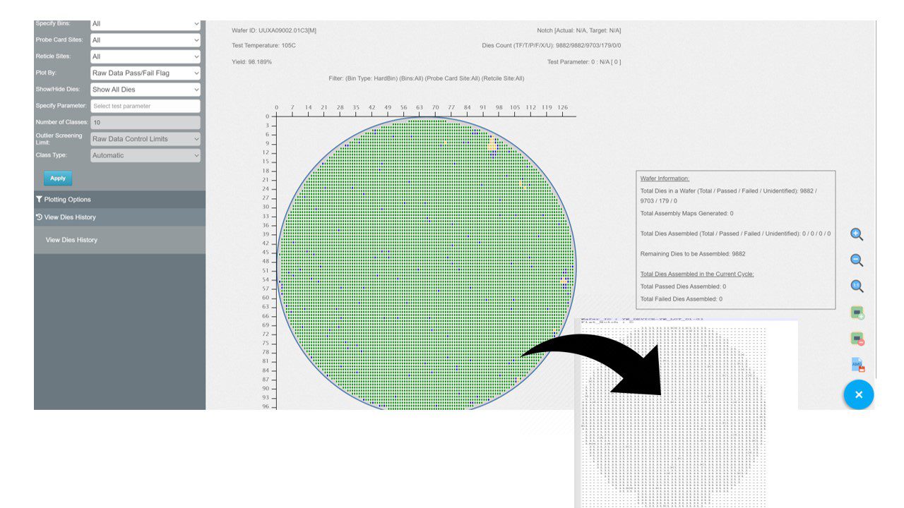
yieldWerx offers the functionality to manually scrap or downgrade die, as well as selectively pick dies from wafers, enabling tracking to specific assembly lots rather than selecting an entire wafer. This capability is particularly beneficial for low-volume applications in the Aerospace and Defense sectors. Users can ‘Re-bin’ die according to custom limits or other business rules defined based on the data collected throughout the wafer’s genealogy. Each ‘Picked Map’ is systematically saved within yieldWerx to facilitate historical reference and audit compliance. 

Value-Added Benefits

  • Unified data combines data from wafers, packaged die, and system boards for holistic view to help identify correlations that may impact yield 
  • Enhanced decision-making by tracking performance metrics across all production tages 
  • Comprehensive root cause Identification correlates failure across testing phases 
  • Improved efficiency by reducing time and complexity in data analysis 
  • Continuous Improvement and ongoing refinement of manufacturing practices through data trends for enhanced quality and better yield rates  
  • Empowers IDM’s to optimize operational efficiency and enhance quality 
Wafer Banks, Screening AND Grading

Advanced Packaging and Board Management

Advanced Packaging and Board Management

yieldWerx enables the collection and analysis of Serialized System and Board data, ensuring traceability from the System and Board level to the Packaged Die and throughout the entire product lifecycle. This integrated tool streamlines the testing process by allowing engineers and quality assurance teams to evaluate data across various production stages simultaneously to identify correlations that may impact yield. 

Value-Added Benefits

  • Comprehensive collection of serialized data for stronger correlations 
  • Streamlined testing by allowing quality assurance teams to evaluate data across production stages 
  • Unified data combines test results from board and packaged die across lifecycle to identify correlations impacting yield 
  • Enables timely intervention based on performance metrics 
  • Thorough root cause identification from failure data across test phases 
Success Popup Widget
PTC-Logo

PTC

Partner

PTC is a semiconductor consulting firm based in Malaysia, providing strategic and technical consulting services to semiconductor manufacturing, assembly, test, product and ecosystem companies across Asia. yieldWerx, a leading innovator in semiconductor yield management solutions, and PTC, a premier Malaysia-based consulting firm for the semiconductor manufacturing industry, have announced a strategic collaboration to address the growing need for comprehensive data analytics across the semiconductor manufacturing lifecycle in the rapidly expanding markets of Malaysia and India.
This collaboration combines yieldWerx’s state-of-the-art analytics platform with PTC’s extensive industry knowledge and regional presence to strengthen semiconductor manufacturing capabilities across East Asia. By providing sophisticated analytics solutions tailored to regional needs, yieldWerx and PTC aim to streamline factory setup and operations, implement rigorous quality assurance protocols, and accelerate the development of sustainable semiconductor ecosystems across both countries. PTC will act as the regional consulting partner, offering advisory, deployment support, and strategic integration services to fabless clients, OSAT facilities, and manufacturing startups adopting the platform.