Products

Efficient NPI Characterization to Accelerate Time-to-Market

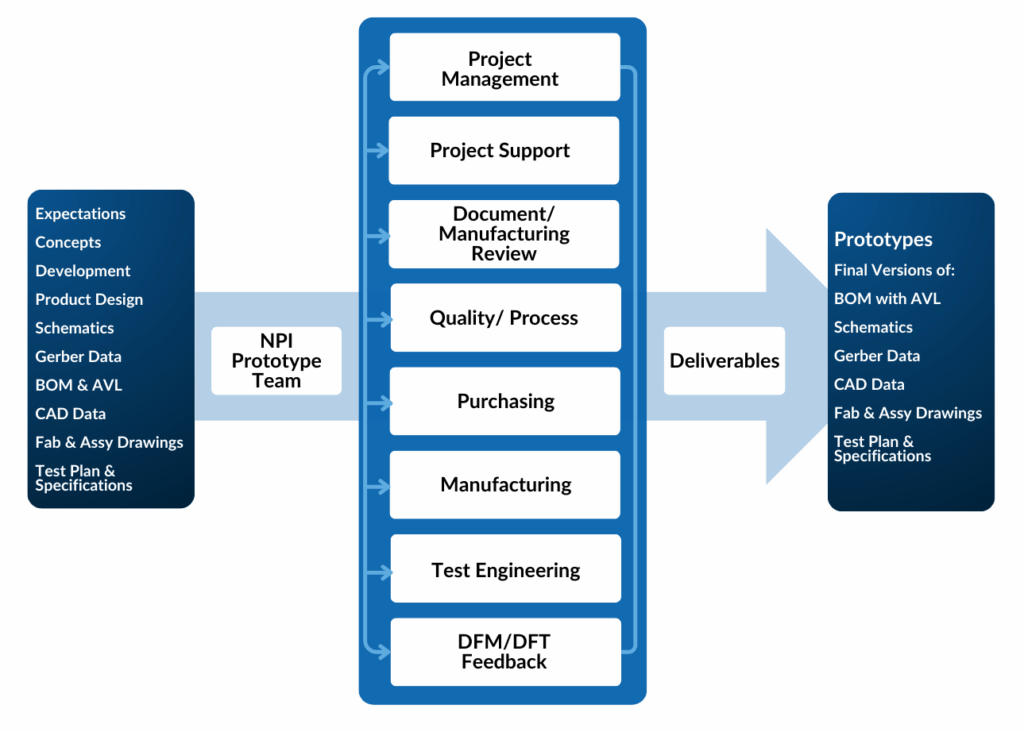
Accelerate your time to market for New Product Introduction with rapid characterization reports, Gage R&R, split lot analysis, drift analysis and identify design sensitivities early and prevent costly re-spins.

What is NPI?

During the New Product Introduction stage of a product, time is paramount. Designs need to be quickly and thoroughly validated to prevent yield loss and inconsistencies.

Early Defect Detection

Identify early-stage defects and inconsistencies

Accelerate Time to Market

Validate and test designs quickly with rapid feedback loops

Design Validation

Rapid characterization reports identify design flaws and viability

Initial Yield Optimization

Forecast yield and mitigate risks and inefficiencies

How It Works

How yieldWerx Streamlines 
NPI

From collecting data across a broad range of systems and sources to cross correlation analytics and making sense of the data points via reports visualizations, yieldWerx provides an unparalleled advantage.

Quality Control & Risk Containment

Quick setup for Characterization Reports, Gage R&R, Device Shift, MVPAT with real-time alerts 
Full 24/7 Test control with data collection, monitoring, binning, statistics

Automated Analysis & Dispositioning​

24/7 Lights out data acquisition across various sources connecting inspection images to data and constructing memory maps for failures

Root Cause Knowledge Graphs

AI-driven knowledge graphs help identify root causes by visually guiding users through weighted paths to identfiy root causes quickly and accurately

Defect Data Management

Intuitive image guided correlation analysis connecting defects to Parametric, Bin, Bin sort and other parameters

Real-Time Machine Control and Monitoring

Provides real-time yield monitoring, OEE, and control of equipment, including probers and handlers, ensuring identifying potential failures before they lead to yield loss

Multidimensional Wafer Merge

Enables split Lot Analysis to apply unique policies and characteristics on merged data sets

Custom Limits Manager

Perform accurate what-if analysis on custom datasets with flexible binning
NPI

Benefits

Why yieldWerx is the Ideal 

Solution
for NPI
Features Section
Rapid Characterization and R&R
Robust Characterization and Gage R&R reports
AI powered Defect Knowledge Graphs
Leverage AI to help with precision defect analytics down to design flaws
Datasets for Shared Analysis
Cross-correlate defect and statics on custom datasets
Advanced Reporting Visualizations
Image-guided visualizations for data-driven actions

Sharpen Your Competitive Edge

Discover the yieldwWerx difference and revolutionize your semiconductor operations. Schedule a demo today!

Success Popup Widget
PTC-Logo

PTC

Partner

PTC is a semiconductor consulting firm based in Malaysia, providing strategic and technical consulting services to semiconductor manufacturing, assembly, test, product and ecosystem companies across Asia. yieldWerx, a leading innovator in semiconductor yield management solutions, and PTC, a premier Malaysia-based consulting firm for the semiconductor manufacturing industry, have announced a strategic collaboration to address the growing need for comprehensive data analytics across the semiconductor manufacturing lifecycle in the rapidly expanding markets of Malaysia and India.
This collaboration combines yieldWerx’s state-of-the-art analytics platform with PTC’s extensive industry knowledge and regional presence to strengthen semiconductor manufacturing capabilities across East Asia. By providing sophisticated analytics solutions tailored to regional needs, yieldWerx and PTC aim to streamline factory setup and operations, implement rigorous quality assurance protocols, and accelerate the development of sustainable semiconductor ecosystems across both countries. PTC will act as the regional consulting partner, offering advisory, deployment support, and strategic integration services to fabless clients, OSAT facilities, and manufacturing startups adopting the platform.