Industries

Accelerating Large-Scale, Complex Photonics Data for Optical I/O Solutions

yieldWerx serves as the enterprise platform for high-quality photonics manufacturing data, spanning wafer probe, optical wafer acceptance test (OWAT), electrical wafer acceptance test (EWAT), module and device assembly, burn-in, and final system test. The platform manages raw data and produces enriched, post-processed results including PAT, virtual binning using custom optical/electrical limits, GDBN/GDBN-Z, multisite merging, multi-insertion merging, and automated pick-map generation. These analytics-ready outputs become the foundation for Design of Experiments (DoEs), parametric optimization, and custom analytics pipelines in photonics manufacturing and optical I/O.

Photonics & LED Manufacturing
Navigating the Complexities of the Photonics Industry:

As photonics moves from R&D to high-volume manufacturing, the challenge is no longer generating data — it is turning highly heterogeneous photonic, optical, and electrical test data into clean, contextualized information that teams can trust. yieldWerx enables this shift by providing a unified data model, automated enrichment, and analytics that operate across wafers, modules, systems, and field-return data. This is exactly where yieldWerx is helping leading photonics companies today.

Photonics & LED Manufacturing 01

Key Challenges

Bridging Fragmented Data into Usable Insight

Multiple test domains, formats, and vendors create fragmentation that prevents rapid, confident decision making.

Achieving True End-to-End Visibility

Siloed systems obscure traceability from wafer probe through assembly and final verification, slowing yield learning and root-cause analysis.

Replacing Manual Analytics with Scalable Workflows

Manual scripts and one-off analyses cannot keep pace with high-volume photonics manufacturing and evolving device architectures.
Our collaboration with yieldWerx gave us measurable results in just 30 days. Their platform ingested our complex photonics data, and the insights have accelerated how we make yield and quality decisions.
— Garth Thompson, CIO, Ayar Lab

How It Works

How yieldWerx Supports
the Photonics Industry:

Comprehensive Quantitative Analysis

Evaluate spectral performance, insertion loss, BER, power, wavelength stability, color/brightness where applicable; supports PAT, PCA, and DOE-ready datasets.

Robust Statistical Process Control

Monitor optical and electrical results across lots and insertions; supports GDBN/GDBN-Z for early deviation detection.

Defect & Image Data Correlation

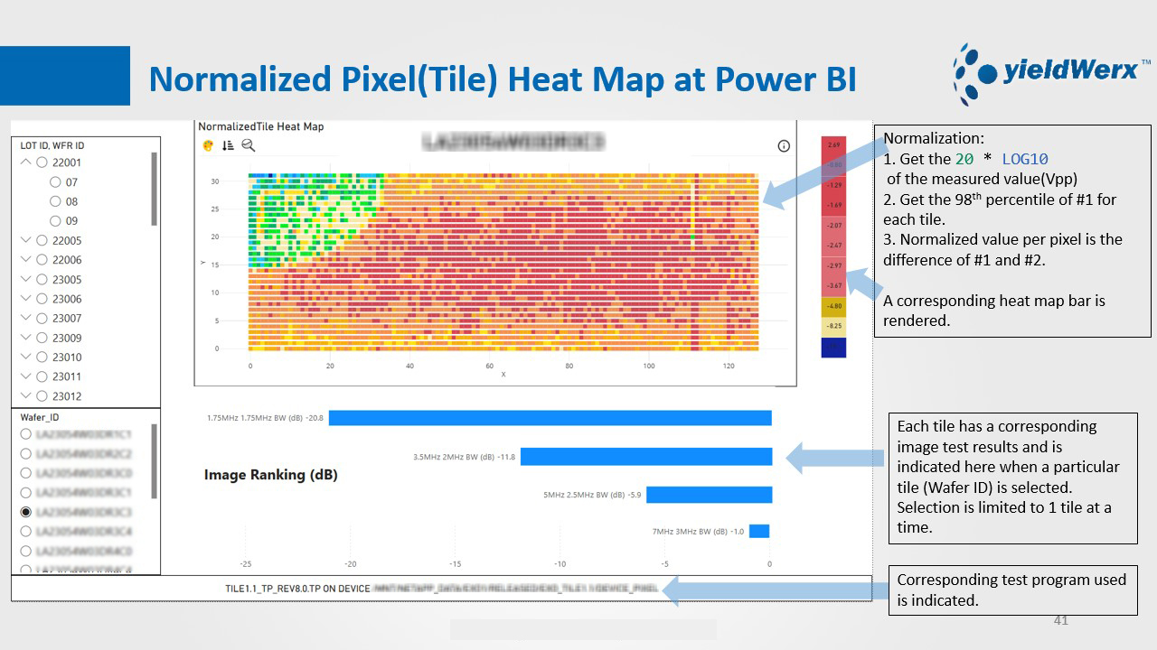
Overlay inspection images and defect maps with OWAT/EWAT outcomes and die locations; supports automated pick-map generation.

Unified Data Repository

Harmonize wafer probe, OWAT/EWAT, assembly, burn-in, final test, and field-return data; supports pixel-, die-, site-, and module-level correlation.

Process & Yield Analytics

DOE, PCA, ANOVA, T-Tests, correlation, commonality, and parametric analysis to accelerate yield ramp and device optimization.

Automated Analysis & Dispositioning

Merge wafers/modules using configurable rules and policies to reduce variability and engineer touch time.

Quality Control & Risk Containment

Advanced outlier control, PAT++, and predictive risk scoring with virtual binning using optical/electrical limits.

AI-Powered Commonality & Root-Cause
Analysis

AI/ML knowledge graphs identify recurring failure signatures across process tools, lots, or designs.

Auto Lot Disposition

Compare cross-lot performance and environmental factors to recommend data-driven disposition policies.

End-to-End Lifecycle Traceability

Wafer → die → coupon → module → final system mapping with genealogy reporting and audit readiness.

Customer Story

A leading U.S. photonics company selected yieldWerx for its ability to rapidly deploy a true end-to-end solution. In just 30 days, yieldWerx ingested heterogeneous photonics data sources, implemented wafer-to-module-to-system traceability, enabled automated PAT/GDBN workflows, and delivered production-ready dashboards and DOE-ready datasets. The decision was driven by our configurable platform, speed-to-value execution model, and deep domain expertise in photonics and optical I/O manufacturing.

Want to learn more?

YieldWerx offers free webinars and downloadable resources covering functionality, data formats and standards, lessons learned, and best practices to elevate your photonics solutions. Sign up below to access these materials and build the foundation to scale your innovation.

Success Popup Widget
modus_test_img

Modus Test

Partner

Modus Test, LLC was founded on the idea that there are creative ways to improve results by combining innovation with the best known methods in test design and manufacturing. Providing innovative test solutions include the MPT series of parametric test and systems and accessories.
Modus Test has a global presence and the capability to support customers in all the IC development centers and high volume manufacturing sites around the world. See for yourself how combining innovation with best-known methods can improve your results.
PTC-Logo

PTC

Partner

PTC is a semiconductor consulting firm based in Malaysia, providing strategic and technical consulting services to semiconductor manufacturing, assembly, test, product and ecosystem companies across Asia. yieldWerx, a leading innovator in semiconductor yield management solutions, and PTC, a premier Malaysia-based consulting firm for the semiconductor manufacturing industry, have announced a strategic collaboration to address the growing need for comprehensive data analytics across the semiconductor manufacturing lifecycle in the rapidly expanding markets of Malaysia and India.
This collaboration combines yieldWerx’s state-of-the-art analytics platform with PTC’s extensive industry knowledge and regional presence to strengthen semiconductor manufacturing capabilities across East Asia. By providing sophisticated analytics solutions tailored to regional needs, yieldWerx and PTC aim to streamline factory setup and operations, implement rigorous quality assurance protocols, and accelerate the development of sustainable semiconductor ecosystems across both countries. PTC will act as the regional consulting partner, offering advisory, deployment support, and strategic integration services to fabless clients, OSAT facilities, and manufacturing startups adopting the platform.