
For over 75 years, silicon has been the dominant material in the evolution of modern electronics, powering everything from smartphones to satellites. But as chipmakers push toward smaller nodes, higher power efficiency, and quantum-scale precision, a pressing question is echoing across fabs and R&D labs worldwide: Is it time to move beyond silicon?
In this blog post, we explore the growing need to rethink our reliance on silicon, not as a trending industry topic, but from the perspective of material performance, sustainability, and manufacturing feasibility. As next-generation applications demand more than what silicon can offer, alternative materials are stepping into the spotlight.
We’ll explore the reasons driving the shift beyond silicon, take a closer look at the emerging materials poised to take its place, and unpack the real-world challenges they’re designed to address in modern semiconductor manufacturing.
We’ll be discussing the following types of materials
Wide Bandgap compound semiconductors for charging speed
- Materials for High-efficiency, High-voltage applications
- 2D materials with tunable bandgaps
- Materials with exceptional strength, conductivity, and flexibility
- Materials with the highest efficiency
Lastly, we’ll discuss the importance of investing in end-to-end yield management solutions that can bridge the gap between scalable operations and experimentation. If you’re in semiconductor design, optoelectronic yield analytics, materials R&D, or just curious about what comes after Moore’s Law—this is a must-read.
Contact us today to learn how our photonics yield analytics platform can help you navigate the transition to next-generation compound semiconductors.
Why Do We Even Need to Replace Silicon?
Modern power systems such as electric vehicles, high-efficiency power supplies, and renewable energy systems demand faster switching speeds, higher voltage tolerance, and better thermal efficiency than silicon can deliver.
For decades, Moore’s Law—the observation that the number of transistors on a chip doubles roughly every two years—has driven the exponential growth of computing power. This remarkable pace of advancement has largely been fueled by the continuous shrinking of silicon transistors, enabling chips to become smaller, faster, and more energy-efficient with each generation.
However, silicon is now approaching both physical and economic limits, and the momentum behind Moore’s Law is beginning to slow—if not stall entirely. On the physical side, scaling transistors below 5nm introduces a host of challenges rooted in quantum mechanics.

Quantum tunneling causes electrons to leak through increasingly thin gate oxides, short-channel effects reduce control over transistor switching, and heat density becomes harder to manage as more transistors are packed into smaller areas. These issues make silicon miniaturization more complex and less reliable.
Economically, the situation isn’t much better. The cost per transistor, which traditionally decreased with each new node, has now plateaued—or even increased—in part due to the extreme complexity of EUV lithography, advanced packaging, and multi-patterning techniques required at leading-edge nodes.
What Are the Top Materials Being Experimented As Silicon Replacement?
Wide Bandgap Materials
Source: Power Electronics News
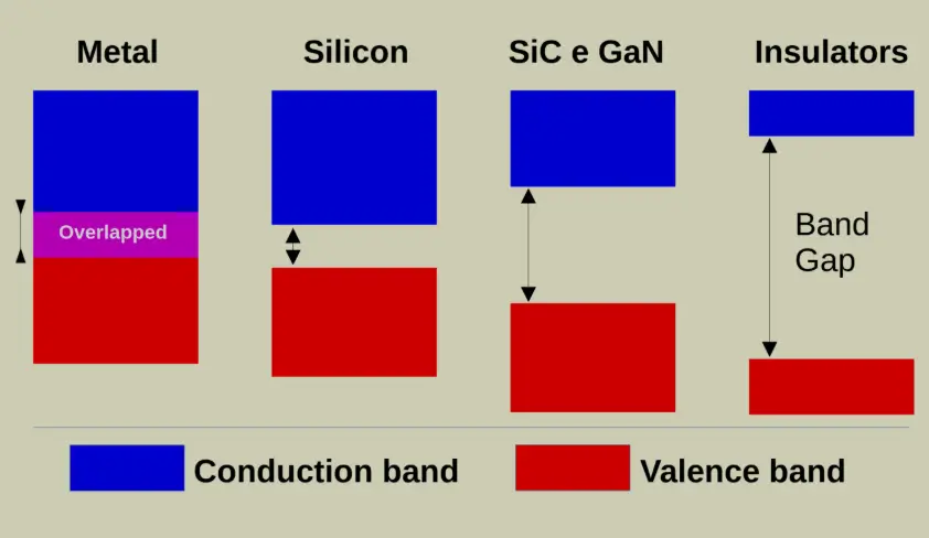
To overcome these issues with silicon, wide-band gap (WBG) materials are seeing fast adoption by both the industry and academia. WBG materials are a class of semiconductors that have a larger energy gap between the valence band (where electrons reside) and the conduction band (where electrons can move freely).
In simpler terms, the wider the bandgap, the better a material can resist electrical breakdown and operate in extreme environments without overheating or losing efficiency. As a result, WBG materials like Gallium Nitride (GaN) and Silicon Carbide (SiC) are becoming key enablers in industries that demand high power, speed, and thermal performance.
The WBG market is projected to be worth USD 5 billion by the end of 2032, as per a recent study by Global Market Insights. Wolfspeed’s silicon carbide and gallium nitride chips are now used in a wide range of devices. With applications rapidly growing, Wolfspeed’s revenue increased by 40% last fiscal year. The company is also building a new silicon carbide chip factory, set to open in 2030, which will increase production by tenfold.
Gallium Nitride (GaN)
Gallium Nitride (GaN) has become the preferred material in fast-charging technology. Modern laptop and smart phone charger ICs are seldom made of any other materials. With its exceptional properties, GaN addresses many of the limitations of traditional silicon, enabling devices that are more efficient, smaller, and capable of faster charging speeds.
It can operate at higher frequencies and switch faster than silicon-based devices. This higher switching frequency reduces switching losses and energy dissipation, making GaN-based chargers much more compact.
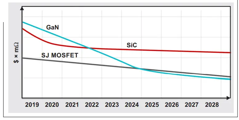
Relative cost projection by FET technology
While Silicon Carbide (SiC) is preferred for very high-voltage applications due to its better performance and efficiency, it is expensive and requires specialized equipment. GaN, on the other hand, offers many of the same benefits and can operate at higher switching speeds. Its lower production cost—thanks to its ability to be grown on silicon substrates—makes it an attractive option, particularly at lower voltages (up to 500V), where GaN can outperform silicon-based technologies.
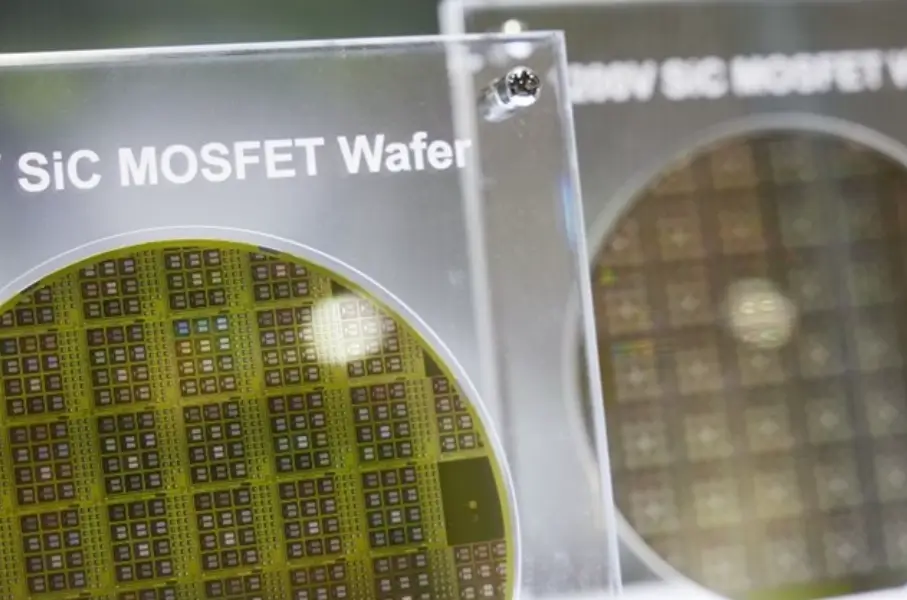
Silicon Carbide (SiC)

Tesla Model 3 Traction Converter made with SiC MOSFETs
SiC is ideal for demanding applications such as electric vehicles (EVs), solar inverters, and industrial power supplies, where efficiency, durability, and heat management are critical. Additionally, SiC exhibits higher thermal conductivity than silicon, enabling it to dissipate heat more effectively and operate under extreme temperature conditions without overheating.
Another key advantage of SiC is its greater efficiency compared to silicon-based IGBTs/MOSFETs in high-voltage applications. SiC power devices experience lower switching losses and conduction losses, leading to improved energy efficiency and reduced system energy consumption.
The result is smaller and more compact systems, as SiC devices can replace bulky and inefficient components, making them particularly attractive in automotive applications and in sectors where space and weight are critical, such as aerospace and defense.
Tesla began using silicon carbide in its inverters in 2018—components that convert DC to AC and power the vehicle. Since then, interest in SiC has skyrocketed within the automotive industry. Today, electric vehicles account for up to 70% of the SiC market, and this key application is poised to drive its adoption in other sectors as well.
While SiC offers numerous benefits, it does have some shortfalls that limit its broader adoption. One of the main challenges is the high cost of production. The manufacturing process for SiC is more complex and costly than silicon, mainly due to challenges in growing high-quality crystals and producing large Silicon Carbide wafers. The raw material and specialized equipment required further increases costs, making SiC devices significantly more expensive than silicon-based alternatives.

Additionally, SiC’s material properties present challenges in device fabrication. For instance, the lattice mismatch between SiC and silicon substrates can lead to defects in the final product. While significant progress has been made in improving SiC production techniques, including advances in epitaxial growth and wafer bonding, there are still issues related to yield and consistency in the production of high-quality SiC devices. Moreover, SiC devices require specialized packaging to handle the heat and voltages they deal with, which adds to the overall cost and complexity of the product.
Finally, although SiC is ideal for high-power and high-voltage applications, it lacks the versatility and scalability of silicon in some low-voltage, low-power applications.
2D Materials
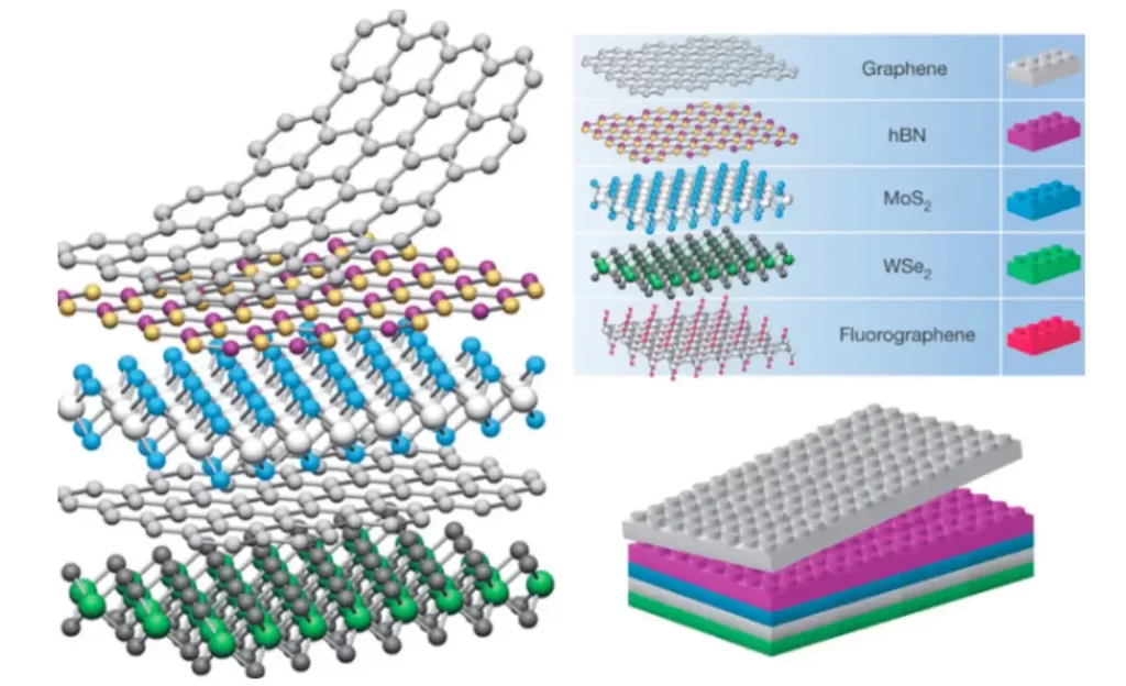
Schematic diagram of a hetero-structured 2D material.
2D materials are pushing the limits of miniaturization and enabling innovations in flexibility, speed, and photonics, but face challenges in manufacturing and integration. As the demand for smaller, faster, and more energy-efficient devices increases, 2D materials are becoming increasingly important, potentially complementing 3D materials in the future. Here we’ll discuss a few of them.
What are Transition Metal Dichalcogenides (TMDs) ?
TMDs are two-dimensional (2D) materials that offer a high surface-area-to-mass ratio and possess unique electronic and optical properties. They represent an exciting class of materials that are gaining attention as potential alternatives to silicon, particularly in the field of nanoelectronics, optoelectronics, and sensing.
Monolayers of materials like Molybdenum disulfide (MoS₂), Tungsten diselenide (WS₂), and Hafnium disulfide HfS₂ exhibit direct and tunable bandgaps, which makes them ideal for transistor fabrication and optoelectronic devices such as light-emitting diodes (LEDs) and photodetectors.
Silicon, on the other hand, only exhibits an indirect bandgap, which means it cannot efficiently emit light or be used for photonic devices. This makes TMDs more suitable for high-performance electronic and photonic devices, which is critical for applications in 5G communication, solar energy, and biomedical imaging.
Overall, TMDs show great promise as alternatives to silicon, but they face several challenges. These include difficulties in scalable production and integrating them into existing semiconductor processes. Additionally, there is a lack of standardization in their use and issues with device stability.
Graphene
First fully functioning Graphene chip Source: New Scientist
Graphene is a one-atom-thick layer of carbon atoms arranged in a hexagonal lattice. Yes, remarkably it is just one atom thick!
It is the thinnest material known to humanity, yet incredibly strong—approximately 200 times stronger than steel. In addition to its remarkable strength, graphene is an excellent conductor of both heat and electricity, and it has unique light control properties, especially at a tiny scale.
Graphene holds significant potential to revolutionize electronics. With its extremely high charge carrier mobility due to no bandgap, it offers performance and strength that far exceed silicon’s capabilities. Its unique properties make it an ideal candidate for applications in wearable electronics, flexible displays, and high-performance transistors.
The widespread adoption of graphene won’t happen unless its production becomes scalable and affordable for real-world chip manufacturing. Scientists need to be able to grow or transfer high-quality graphene onto wafers at scale, and for a long time, this wasn’t possible.
But now, it’s starting to change. New graphene fabs are being built around the world, such as Black Semiconductor’s FabONE in Germany, which plans to begin production in 2026 and scale up to full volume by 2030.
Graphene is often grown on materials like copper or silicon carbide, but moving it onto a chip-ready surface without cracks, defects, or contamination is still a major challenge. Before graphene can power entire computing systems, it will first make its impact in interconnects, and that’s where we’re likely to see the first real-world applications.
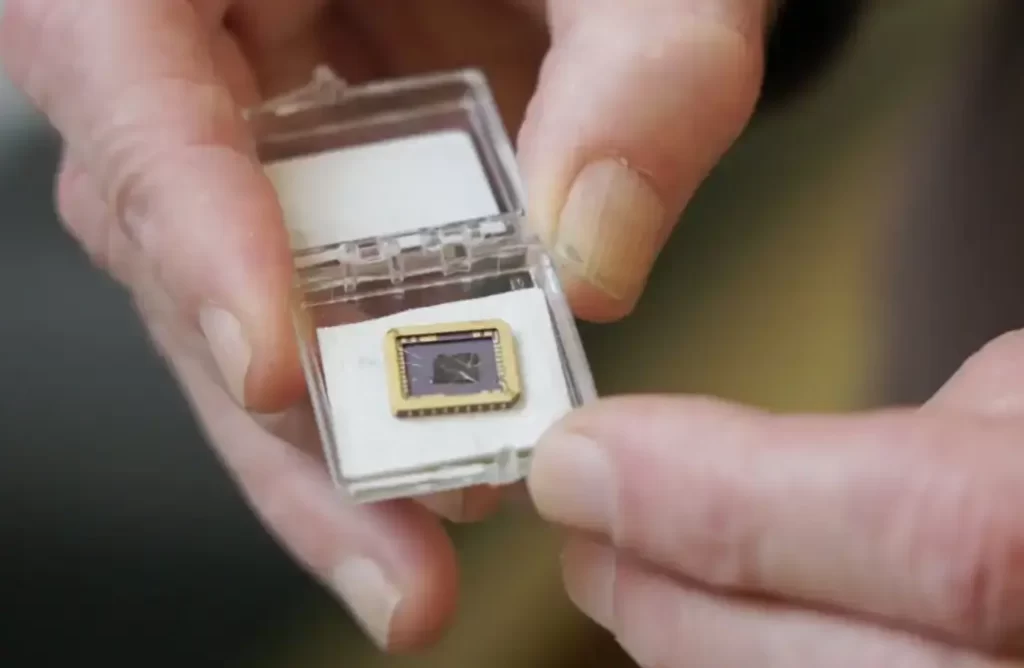
Bismuth
A groundbreaking paper published in Nature introduces the first bismuth-based microchip, operating at the Ångström node (0.1 nm). Bismuth, a 2D material, has unique quantum properties like strong spin-orbit coupling, allowing for better control over electron spin and charge, making it ideal for next-gen electronics. The material used in this study is Bi2O2Se (Bismuth OxySelenide).
However, bismuth lacks a natural bandgap, making it act more like a metal than a semiconductor. The solution lies in doping it with bismuth telluride, turning it into a perfect semiconductor. Bismuth-based transistors operate at 500GHz, a 100x increase over silicon’s 5GHz.
Tests against Intel, TSMC, and Samsung chips show that bismuth is 40% faster and three times more energy-efficient. With graphene interconnects pushing speeds up to 10GHz, this breakthrough could shape the future of semiconductors. However, scaling and integrating bismuth into mass production remains a challenge.
How soon can Silicon be replaced in semiconductor chips?
Blanket replacement of silicon in the semiconductor industry may not be possible. However, in the next 10-15 years, we can expect to see stacking and hybrid integration technologies evolve, with newer semiconductor material layers being commonly added on top of silicon-based chips, making processors more compact, faster, and efficient. Overall, next-gen semiconductors are surely set to become the backbone of modern technologies.
How yield management platforms help companies transition to compound semiconductors?
As Fabs develop processes and manufacturing tools around these new materials, scalable and flexible data analytics tools will be critical in the adoption. From a yield management perspective, it will be critical for companies to focus on optimizing the integrated photonic yield of these new materials during early-stage production. The complexity of mixed materials will increase the risk of defects and variations, making traceability and defect detection systems essential.
Disconnected MES and SPC tools create data silos, preventing enterprises from gaining a centralized view of their production. Without cross-functional alignment through unified analytics platforms, performing root cause analysis and optimizing yield becomes a significant challenge.
Unified yield management systems like yieldWerx are made exactly to break down these silos, improve traceability and reduce yield losses.
Book a Demo to get first-hand experience of how yieldWerx can streamline the semiconductor manufacturing and optoelectronic semiconductor analytics, delivering precision and efficiency every step of the way.
Related Blog Posts:


