The conversations around Artificial Intelligence inevitably lead to a discussion about chips. From boardrooms to tech conferences—and even in speeches by world leaders—AI chips have become the center of attention. The reason is straightforward: without specialized chips, even the most sophisticated algorithms and ambitious AI applications remain just ideas on paper. But here’s where things get interesting. Not all chips are created equal. While traditional processors like CPUs and even GPUs have powered the digital world for decades, AI chips operate with a very different set of design principles.
In this post, we’ll break down AI chips vs traditional chips and explore what makes AI chip architecture unique. We’ll also go a step further by looking at the growing ecosystem of AI chips—GPU, TPU, NPU, FPGA, and ASICs—and why each matters in its own way. On top of that, we’ll talk about the enormous power requirements for AI datacenters and what that means for companies thinking about jumping into AI chip production.
Spoiler: It’s not just about designing silicon—it’s about planning for an entirely different set of inputs, from energy to infrastructure.
Understanding the difference between AI chips vs regular chips isn’t just for those in the technology industries—it’s for anyone who wants to see where the next wave of opportunity in semiconductors is headed.
CPU vs GPU vs TPU vs NPU vs FPGA vs ASICs
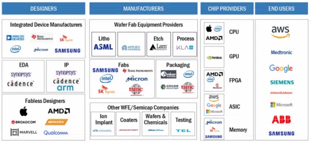
AI Chip Industry Ecosystem – Source: Markets&Market.com
From general-purpose CPUs to specialized AI accelerators like GPUs, TPUs, NPUs, FPGAs, and ASICs, each custom chip is built with different strengths. Some are flexible, others are fast or energy-efficient, and some are purpose-built for very specific tasks. Here’s how they compare.
CPU: The General-Purpose Workhorse
The CPU, or central processing unit, is the foundation of every computer system. Designed with only a handful of powerful cores, it excels at sequential processing—tackling one task at a time with precision. This makes CPUs incredibly versatile, capable of running operating systems, applications, and even small-scale AI workloads. However, when faced with massive datasets and the parallel math required for training AI models, CPUs quickly run into bottlenecks. They are flexible and programmable but not optimized for the repetitive, data-heavy calculations that dominate artificial intelligence. Intel leads this market followed by AMD.
GPU: The Parallel Processing Powerhouse
GPUs, or graphics processing units, transformed AI by making large-scale parallelism practical. With thousands of smaller cores, GPUs break complex problems into many smaller ones and solve them simultaneously. Originally built for rendering graphics, they have become the go-to chip for machine learning and deep learning because of their speed in handling matrix multiplications. The trade-off is energy consumption—GPUs are powerful but power-hungry, requiring substantial infrastructure in data centers. They remain the backbone for AI training and high-performance computing where scalability and raw power are essential. Nvidia dominates this sector with 92% share followed by AMD. Nvidia H100 and RTX 5090 are considered the top-tier GPUs for AI.
TPU: Google’s AI Specialist
The Tensor Processing Unit (TPU) is Google’s answer to the growing demand for AI acceleration. Unlike GPUs, which balance between graphics and AI, TPUs are laser-focused on tensor operations—the mathematical backbone of neural networks. They excel at training and inference for large language models and deep learning systems. By stripping away features unnecessary for AI, TPUs deliver superior efficiency compared to GPUs in many cases. However, their availability is limited, as they are tightly integrated into Google’s ecosystem, primarily through Google Cloud.
NPU: Brain-Inspired Efficiency
Neural Processing Units (NPUs) are built to mirror how the human brain processes information, with a strong focus on data flow and memory hierarchy. This design allows them to deliver highly efficient, real-time inference while performing thousands of parallel operations simultaneously. Their strength lies in powering large language models (LLMs) and handling multimedia workloads such as speech recognition, image classification, and AI-driven video features.
Because they combine parallelism with low power consumption, NPUs are especially valuable in IoT devices like smartphones and wearables, where battery life is critical. In data centers, they help optimize resources for heavy AI workloads, while in autonomous vehicles and robotics, they enable fast computer vision and real-time decision-making. Unlike GPUs, which are powerful but energy-hungry, NPUs achieve comparable levels of performance with far greater efficiency, making them a natural fit for both edge devices and consumer applications. Qualcomm and Intel NPUs are typically combined with GPUs to offload the more demanding AI tasks.
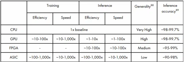
Comparing AI chips to CPUs. Source: AI-Chips What They Are and Why They Matter
FPGA: The Adaptable Accelerator
Field-Programmable Gate Arrays (FPGAs) offer a unique middle ground in the AI chip landscape. Unlike fixed-function chips, FPGAs can be reprogrammed after manufacturing to suit specific AI models or workloads. This flexibility makes them particularly valuable for prototyping and adapting to evolving algorithms.
While they may not match ASICs or TPUs in raw efficiency, their ability to be tuned for different applications allows organizations to keep pace with AI’s rapid innovation cycle. They are often used in telecommunications, edge AI, and industries requiring deterministic, low-latency processing. Top manufacturers include Intel, AMD and Gowin Semiconductors.
ASICs: Maximum Efficiency, Minimum Flexibility
Application-Specific Integrated Circuits (ASICs) represent the pinnacle of specialization. These chips are custom-built for one task—whether that’s powering a search engine, enabling face unlock on a phone, or running recommendation systems in a data center. Because they are designed for a narrow workload, ASICs achieve unmatched efficiency and performance, sometimes hundreds of times more energy-efficient than GPUs. The downside is inflexibility: if AI models evolve or workloads shift, an ASIC may quickly become obsolete. This makes them ideal for large-scale companies that can afford to design chips for tightly defined use cases. Leading manufacturers include Cerebras, Google, Intel, Cambricon and Huawei.
What is so special about AI Chips?
AI chips aren’t just faster processors; they are the foundation of modern artificial intelligence.
What makes them so valuable is their combination of speed, scale, and specialization. GPUs opened the door with parallel computing, but more advanced accelerators like TPUs or ASICs can be hundreds of times more energy efficient than GPUs, reducing both cost and environmental impact.
This efficiency matters not just for smartphones and edge devices, but also for AI data centers where the scale of computation is staggering. Without these chips, advanced AI models simply cannot be trained or deployed effectively.
That’s why every country sees AI chips as a strategic resource. Nations understand that semiconductor dominance translates directly into leadership across critical sectors, leading to key breakthroughs in defense systems, cybersecurity, healthcare, finance, and next-generation manufacturing. Just as petroleum fueled the industrial age, AI chips fuel the intelligence age. Controlling them means controlling who gets to lead in AI innovation. For this reason, nations not only compete to design and manufacture AI chips but also guard access through export restrictions, subsidies, and strategic alliances.
In short, AI chips are special because they determine who holds the advantage in the race for artificial intelligence—economically, politically, and technologically.
The Energy Demands of AI
AI’s supply chain is both highly complex and geographically concentrated, stretching from chip manufacturing to massive data centres that power large-scale model training. Companies like OpenAI, Google, Meta, NVIDIA, and Baidu develop models requiring vast datasets, specialised hardware, and immense computing power.
While some AI applications can run “at the edge” (on devices like smartphones or cars), large models are trained and deployed in energy-hungry data centres. For example, training GPT-4 is estimated to have consumed around 42.4 GWh of electricity over 14 weeks—equivalent to the daily usage of tens of thousands of households. Fine-tuning requires less energy, but deployment still demands powerful GPU servers for each user query.
Each time a user interacts with an AI model—such as posing a question to ChatGPT—the system performs billions of calculations to generate a response. These computations run on GPU-accelerated servers used in training. The electricity consumed during this “inference” phase varies widely, depending on factors like the size of the model, the length and complexity of the input and output, the mode of interaction, and the underlying hardware configuration. Energy usage estimates for different AI models can be tracked in real-time using this dashboard.
Chip production adds another layer of intensity: manufacturing a single wafer of a 3 nm chip consumes about 2.3 MWh of energy. For a high-performance server, that’s over 10 MWh just in production—before accounting for more than 80 MWh consumed in operation over five years.
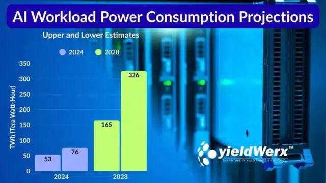
Data centers in the US used somewhere around 200 terawatt-hours of electricity in 2024, roughly what it takes to power Thailand for a year. AI-specific servers in these data centers are estimated to have used between 53 and 76 terawatt-hours of electricity.
By 2028, the researchers estimate, the power going to AI-specific purposes will rise to between 165 and 326 terawatt-hours per year. That’s more than all electricity currently used by US data centers for all purposes. Between 2024 and 2028, the share of US electricity going to data centers may triple, from its current 4.4% to 12%.
How Much Energy Does a ChatGPT Query Use?
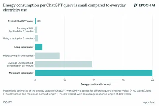
Source: EPOCH AI
A single ChatGPT query consumes far more electricity than a traditional Google search, though the exact amount depends on the model and the request. For lightweight models like ChatGPT or Google Gemini, a typical text reply uses around 0.24 – 0.30 watt-hours (Wh)—about ten times more than a Google search.
Heavier tasks, such as reasoning requests with GPT-5, are far more energy-intensive. Academic benchmarks show that generating a medium-length response of ~1,000 tokens can average 18 Wh, and in some cases spike to 40 Wh. That’s the same as leaving a 60-watt bulb on for 18–40 minutes. Image and video generation models are surely more energy-intensive.
With OpenAI reporting up to 2.5 billion requests per day, ChatGPT’s overall electricity use is estimated at 45 gigawatt-hours (GWh) daily—enough to power 1.5 million U.S. homes. Even limited personal use has a noticeable footprint: a single GPT-4o session can consume about 10 Wh.
The Essential Inputs for Making AI Chips
AI chipmaking isn’t just about etching patterns into silicon; it’s a multifaceted process that combines technical expertise, advanced tools, specialized materials, and substantial financial backing. To even begin developing a competitive AI processor, startups and established players alike need to align several critical inputs.
Building the Right Team
The most critical input in building an AI chip is human capital. It takes a highly specialized and collaborative team to bring such a complex product to life. Talent is by far the scarcest and most valuable resource, which is why so many successful AI chip startups are founded by veterans from Nvidia, Intel, or Apple.
Talent poaching is rampant with reports of some AI experts getting offered hundreds of millions in salaries and other benefits. Onboarding one anchor expert can attract tens of other high-skill engineers.
Many companies have chosen a faster route: acquiring specialized chipmaking companies to instantly gain technology, expertise, and intellectual property. These deals have often been pivotal in positioning companies as leaders in the AI hardware race.
One of the most famous examples is Apple’s acquisition of PA Semi in 2008. At the time, PA Semi was a small chip design firm, but its low-power processor technology became the foundation for Apple’s in-house silicon program. The $278M price for 150+ engineers laid the foundation for all the Apple Silicon chips that have generated over $500B+ in value to Apple.
Other major acquisitions tell a similar story:
- AMD’s $35B purchase of Xilinx (2020):
Strengthened AMD’s position in adaptive computing and FPGAs, critical for AI acceleration and heterogeneous architectures.
- Nvidia’s $6.9B acquisition of Mellanox (2019):
Not a chip design firm, but a networking specialist. This move boosted Nvidia’s data center capabilities, crucial for scaling GPU-based AI systems.
- Amazon’s acquisition of Annapurna Labs (2015):
Provided the foundation for AWS’s custom Graviton CPUs and Inferentia AI chips, which now power many of Amazon’s cloud AI services.
The Cost of Entry
Behind all of this is the financial foundation. AI chipmaking is one of the most capital-intensive ventures in technology, with R&D costs often exceeding $100 million before a viable product reaches market. The process can consume one to two years.
Tape-out costs, EDA licensing, and top-tier engineering salaries add up quickly, creating a steep barrier to entry. Funding usually comes from a mix of venture capital firms, corporate investors, government subsidies, sovereign wealth funds, and strategic partnerships.
Deep-tech VCs like Sequoia, Gaingels, Lux Capital, and specialized funds such as Silicon Catalyst Angels typically back startups that have strong technical teams with proven experience, clear differentiation from incumbents, and early signs of market demand. One example is Normal Computing’s physics-based ASICs designed for efficient computation of linear algebra and matrix operations.
Large technology companies, like Google, Microsoft, and Amazon to Tesla, Apple, and Samsung, may invest if a chip aligns with their own product or cloud strategies, often providing both capital and early adoption.
Governments also play a key role, with programs such as the U.S. CHIPS Act, EU Chips Act, and Asia’s subsidies in Singapore, India, Taiwan, and South Korea, which support national priorities like AI independence and defense. On the financial side, sovereign wealth funds like Saudi PIF, Mubadala, and Temasek, along with players like SoftBank, have invested heavily in semiconductor and AI infrastructure.
Design Tools and Intellectual Property
Equally important are design tools and intellectual property. No chip can be realized without Electronic Design Automation (EDA) tools from vendors like Cadence or Siemens. These tools, which can cost millions of dollars in licensing fees.
They cover every stage of chipmaking — from front-end logic design and simulation, to back-end physical layout, timing, and power analysis, as well as packaging and testability. For AI chips, which can contain billions of transistors, EDA tools reduce risk and prevent costly errors, since a failed tape-out at advanced nodes can waste $10M–$50M.
The US government strictly controls their usage in order to prevent Chinese companies from developing leading-edge chips. Therefore, startups must evaluate geo-political risks before getting locked-in with any vendor.
In addition, chipmakers often rely on pre-designed processor IP cores such as ARM or open-source RISC-V, along with memory and interconnect IP for handling bandwidth-heavy AI workloads. Before committing to fabrication, many companies use FPGA boards to test and refine their architectures.
Fabrication Access

Fabrication access forms the next crucial layer. Since most AI chip companies are fabless, they depend on foundries such as TSMC, Samsung, Intel Foundry Services, or GlobalFoundries. Most of these top foundries have production lines booked for the next several months or even years.
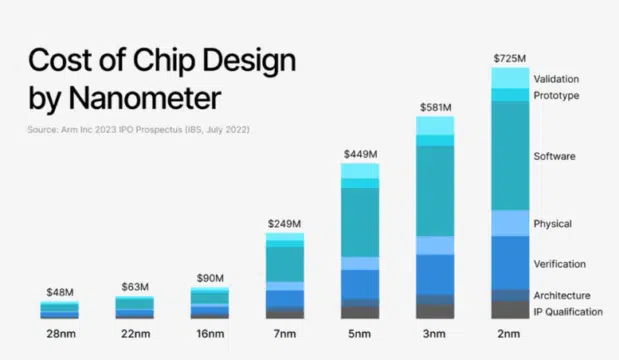
The choice of process node is a key strategic decision. While 7nm, 5nm, and even 3nm are essential for datacenter-class chips, older nodes like 28nm or 16nm can be sufficient for cost-sensitive edge applications. Regardless of the node, tape-out costs are immense, ranging from $5 million for older technologies to $50 million or more at the cutting edge.
Materials and Hardware Infrastructure
The physical materials and supporting hardware also matter enormously. Ultra-pure silicon wafers, high-bandwidth memory stacks, and advanced packaging technologies such as 2.5D and 3D stacking are vital for delivering the performance modern AI workloads demand. Sophisticated testing equipment is equally important to verify yield and reliability before chips can be deployed at scale. AI startups can readily outsource yield management tasks to specialised firms like yieldWerx to cut costs.
Software Ecosystem and Developer Adoption
Just as critical as the hardware is the software ecosystem that surrounds the chip. Even the most powerful processor can fail in the market if developers cannot easily use it. That’s why successful AI chipmakers invest heavily in compilers, SDKs, drivers, and optimization tools.
Compatibility with popular frameworks like PyTorch and TensorFlow is non-negotiable, and developer support often determines whether a chip gains traction. Nvidia’s dominance is owed as much to its CUDA software ecosystem as to its silicon.
Strategic Partnerships for Scale

Nvidia CEO Jensen Huang and TSMC CEO CC Wei doing press conference in Taiwan, Aug/2025
Finally, no chip company succeeds in isolation. Strategic partnerships with foundries, cloud providers, and OEMs are essential. Foundry alliances ensure access to manufacturing capacity, while cloud providers like AWS or Google can serve as both investors and early customers. Partnerships with OEMs in industries such as automotive, robotics, and telecoms provide the deployment channels needed for scaling production.
Nvidia’s CEO Jensen Huang followed a philosophy he called “Rough Justice.” The idea was simple: sometimes Nvidia would win in a deal and sometimes the supplier would, but over time it had to balance out to roughly 50/50. This approach focused on building long-term trust rather than nickel-and-diming suppliers.
What is the future of AI Chips?
The story of AI chips is no longer just about raw performance. While GPUs helped ignite the AI revolution through parallel computing, the future lies in a diverse ecosystem of specialized processors—TPUs for tensor operations, NPUs for energy-efficient edge inference, ASICs for maximum efficiency, and FPGAs for adaptability. Each of these chip types plays a distinct role, and together they form the backbone of next-generation AI systems.
But hardware is at a crossroads. AI models are evolving at a breathtaking pace—sometimes in weeks—while silicon development cycles can take years. This synchronization gap means the old one-size-fits-all approach is unsustainable. The future of AI chips will hinge on flexibility and reconfigurability: modular, chiplet-based architectures that can adapt to new algorithms, minimize energy waste, and bring AI closer to users through edge devices. Neuromorphic and physics-based designs may push this even further, mimicking the efficiency of the human brain or exploiting new physical phenomena to deliver breakthroughs in power savings.
At the same time, AI isn’t just running on chips—it is increasingly designing chips. Reinforcement learning and generative AI are streamlining electronic design automation (EDA), enabling faster design migration, better PPA (power, performance, area) optimization, and reduced time-to-market. This creates a feedback loop: AI accelerates chip design, and better chips accelerate AI.
The takeaway is clear: AI chips are the new strategic resource. They will shape not only the competitiveness of companies but also the technological sovereignty of nations. For businesses, the path forward is to embrace a multi-architecture mindset—matching the right chip to the right workload—while investing in design strategies that prioritize flexibility, scalability, and energy efficiency.
The future of AI won’t be powered by a single breakthrough chip but by an intelligent ecosystem of processors that evolve as quickly as the algorithms they support. Companies that recognize this shift and act now—building partnerships, investing in adaptable architectures, and leveraging AI-driven design—will be the ones to lead in the intelligence-first economy.
Written by M. Rameez Arif, Content & Communication Specialist at yieldWerx.
Edited by Tina Shimizu, Content Strategist at yieldWerx.