From futuristic VR goggles and the glow of red light facial therapy, to the laser-sharp vision of self-driving cars, and the blazing intelligence of AI, these cutting-edge innovations all share one incredible commonality: light. More precisely, the science of photonics. Let’s explore how this transformative technology is already illuminating our world in ways you might not expect.
Discover how yieldWerx can transform your semiconductor test data into smarter decisions and higher yields. Start your journey today by contacting us.
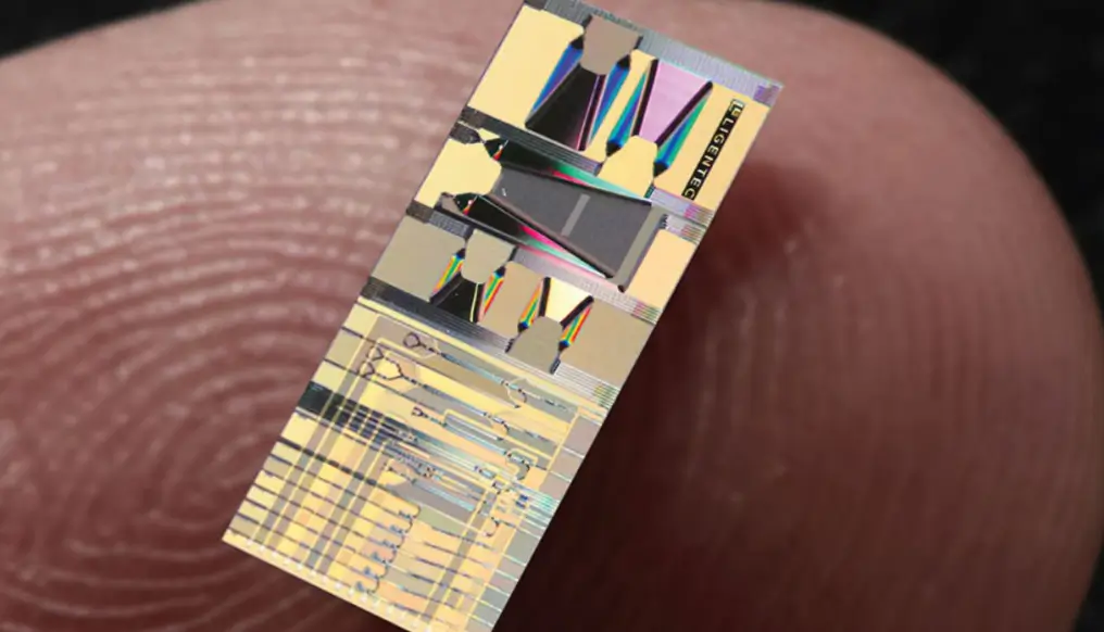
What is Photonics?
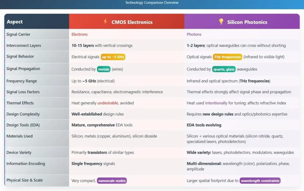
Photonics is the science and technology of generating, controlling, and detecting light— or more precisely, photons. Unlike electronics, which deal with the flow of electrons, photonics focuses on manipulating the properties of light across a broad spectrum, including ultraviolet, visible, and infrared wavelengths. This field encompasses everything from lasers and optical fibers to sensors and medical imaging systems.
Light’s Wave-Particle Duality
At the heart of photonics lies the fascinating quantum phenomenon known as wave-particle duality — the idea that light exhibits both wave-like and particle-like properties depending on how it is observed. Light propagates and interacts in ways best described by wave theory, such as interference and diffraction. Yet, at the same time, it carries energy in discrete units called photons, the quantum particles of light.
This dual nature enables a wide range of photonic technologies. For example, the wave properties of light allow for high-speed data transmission through optical fibers, while its particle-like behaviour is essential for precise detection and sensing at the nanoscale — capabilities that are increasingly harnessed in advanced systems like silicon photonic circuits.
Source: SemiEngineering
What is Silicon Photonics?
Silicon photonics is an advanced technology that integrates optical functions such as generating, modulating, and detecting light directly onto silicon-based integrated circuits. By leveraging standard CMOS manufacturing processes used in traditional semiconductor fabrication, silicon photonics enables the cost-effective and scalable production of photonic integrated circuits (PICs), which can transform high-speed data communication, computing, and sensing technologies.
However, this fabrication technique is not simple and requires sophisticated methods to create waveguides, modulators, and photodetectors that precisely control light within microscopic footprints. Since pure silicon has inherent limitations, particularly its inefficiency in emitting light due to an indirect bandgap, and its limited sensitivity at telecom wavelengths, silicon photonics often incorporates complementary materials to enhance performance. This technology requires specialized materials such as silicon nitride, Germanium and III-V family semiconductors to enhance performance in areas where silicon alone falls short.
Photonics: Illuminating More Than Just Our Homes
Source: American Chemical Society
Photonics plays a vital role in our daily lives — from the LED lights in our homes to the laser diodes in fiber-optic networks that power the internet. These solid-state light sources are compact, durable, and energy-efficient, making them far superior to traditional incandescent or fluorescent lighting. They consume less power, generate less heat, and last significantly longer — offering both economic and environmental benefits.
However, photonics is much more than just illumination. It plays a vital role in enabling ultra-fast communication networks that connect the world, creating highly sensitive sensors that can detect the tiniest changes, and developing advanced imaging systems that improve everything from healthcare to manufacturing. By harnessing the power of light, photonics allows data to be transmitted at lightning-fast speeds with much lower power consumption than conventional electronic systems.
A perfect example of photonics’ impact is the pulse oximeter—a device widely used in healthcare that measures blood oxygen levels non-invasively by analyzing how light passes through the skin. This innovation provides critical, real-time health information without discomfort or risk, highlighting how photonics is transforming medical diagnostics and patient care. Numerous studies have shown that portable oximeters have drastically reduced the number of Arterial Blood Gas Testing which is an expensive and painful procedure.

Another example are the handheld ultrasound devices that integrate photonics technologies, such as pulsed laser diodes and fiber optics, to generate and transmit ultrasound waves with high precision. These photonic components enable compact and high-resolution imaging systems controlled via smartphones.
By combining optical contrast and ultrasound, they deliver enhanced image quality and portability, making them invaluable tools for real-time diagnostics in clinical and remote settings.

Source: Real Time Ultra Sound
“I believe the future of technology will be shaped by how we control light at very small scales, “ says Dr. Hamza Humayun, Physics Lab Instructor at the LUMS university. “Silicon photonics is already improving AI and data communication, but when we combine it with new materials like quantum dots and metasurfaces, we can make devices that are faster, smaller, and more energy efficient. This will lead to big changes in computing, sensing, and renewable energy systems.”
Photonics vs. Optics: What’s the Difference?
Optics is the classical science of light focusing on how light behaves as it travels through lenses, mirrors, prisms, and other components. It’s primarily concerned with guiding, bending, and shaping light for applications like imaging, illumination, and measurement. Think of optics as the foundational tools and principles that control how light moves and interacts with materials, typically on a macroscopic scale.
Photonics, on the other hand, is a broader field that not only includes the manipulation of light but also its generation, modulation, detection, and information processing at very small scales—often integrated directly onto chips. Photonics harnesses photons (light particles) to perform functions similar to how electronics use electrons.
Why do they need to coexist on silicon?
Combining optics, photonics, and silicon has opened the door to transformative advances in computing and communication through silicon photonics. By leveraging the speed of light, photonics enables data to move significantly faster than traditional electronic signals, overcoming the bottlenecks imposed by copper interconnects.
The use of silicon, the backbone of CMOS fabrication, ensures compatibility with existing semiconductor manufacturing processes, allowing mass production at a reduced cost. Silicon’s high refractive index contrast allows tight confinement and miniaturized components, which makes it possible to create complex optical circuits in small footprints.
Integrated photonics comprising components such as lasers, modulators, and detectors directly onto silicon chips results in smaller, faster, and more reliable systems. Beyond communication, silicon photonics is laying the groundwork for cutting-edge applications like quantum computing, LIDAR, and biosensing.
Altogether, the fusion of these three domains marks a pivotal shift in how we design high-performance, future-ready technologies.
How Do Photonic Integrated Circuits Work and What Problems Do They Solve?
Photonic Integrated Circults (PICs) operate by using a laser to inject light into their components, much like how electronic circuits use electricity to power transistors and other elements. But instead of relying on electrons, PICs manipulate photons to transmit and process information. Within a photonic chip, these photons travel through components such as waveguides, lasers, polarizers, and phase shifters.
Some of the commonly-used PICs are listed below:
- Transmitter laser circuits
- Repeater chips
- Optical wavelength demultiplexers
- Integrated tunable receivers
- Distributed feedback lasers and modulators
- Bistable optical devices
What Are the Challenges of Photonics Packaging and Manufacturing?
Manufacturing Challenges
The manufacturing process of silicon photonics starts with imaging and etching passive optical components like waveguides and couplers that guide light on the chip. Modulators convert electronic signals into optical signals by altering light’s intensity or phase, while photodetectors convert optical signals back to electronic form, completing communication.
Waveguides require more intricate designs than traditional electronic circuits because photons travel straight and struggle with sharp bends, which can cause signal loss. Curvilinear masks are used to create smooth, rounded waveguide paths that closely follow the natural trajectory of light, reducing optical losses and improving performance. This enhanced precision allows for more efficient, compact, and densely packed photonic circuits.
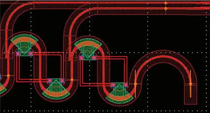
Curvilinear shapes created with Electronic/Photonic Design Automation (EPDA) by Cadence
Packaging Challenges
Photonics packaging is even more complex and costly, requiring precise alignment to maintain signal integrity.
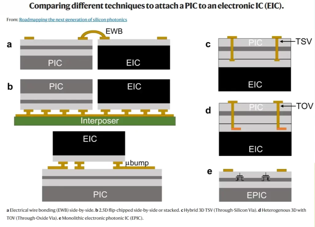
Todd Bermensolo, product marketing manager at Alphawave Semi says, “the question now is how close you can put silicon photonics next to electron components when you’re stacking them on an interposer. As you slam two wafers together, you have to have some kind of interconnect that allows you to stitch them together, like a build-up layer. But that ends up being a very challenging interconnect.”
Some key factors behind such high costs and complexities are:
Precision Alignment
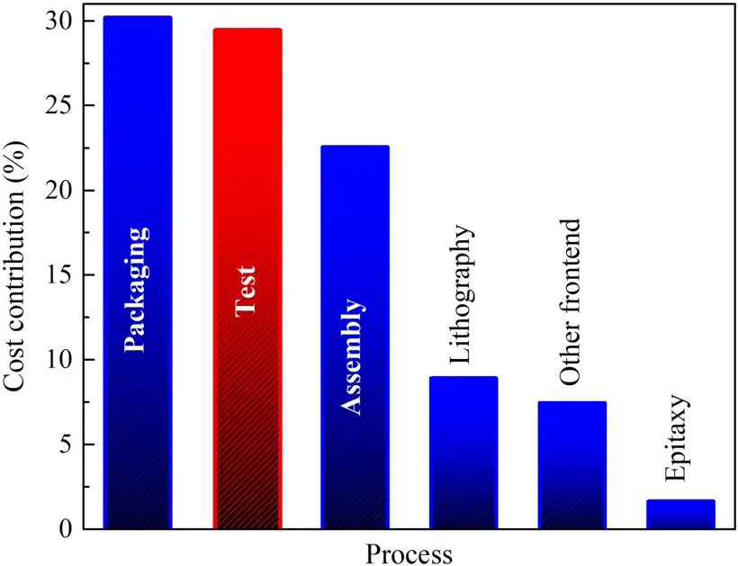
Unlike traditional electrical components, photonic components require precise alignment to maintain signal integrity. The alignment challenge in photonics stems from the need to precisely couple light into photonic circuits with sub-micron accuracy, often within tens of nanometers.
This precision is crucial because misalignment results in significant signal loss (in dB), which cannot be compensated as in electronics due to the absence of amplifiers in most photonic systems. Unlike electronics, photonics demands complex alignment for each optical interface, consuming up to 80% of production costs.
Thermal Management
Photonics circuits are highly sensitive to temperature changes, which can affect their performance. Sophisticated cooling solutions are needed to prevent temperature fluctuations from interfering with optical transmission.
Material Compatibility
Photonics components often require specialized materials that are optimized for optics, not for thermal expansion. Mismatches in the thermal expansion properties of materials (CTE mismatch) can lead to mechanical stress, making it more difficult and costly to maintain stable operation over time.
Integration Complexity
The integration of photonic and electronic components on the same chip is complex. This process requires advanced fabrication techniques, including the deposition of various materials and the creation of sophisticated waveguides and modulators.
Testing and Quality Assurance
Both electronic and optical testing are necessary to ensure the integrity of signal paths and the performance of photonic devices. This testing process is detailed and expensive, as it involves scrutinizing waveguides for optical losses, evaluating modulators and detectors for efficiency, and assessing the overall data transmission capabilities.
Source: Open Standards for Automation of Testing of Photonic Integrated Circuits
What are Co-Packaged Optics?
Co-packaged optics refers to the integration of optical components directly into the same package as the electronic components, such as the processing unit (e.g., a chip or processor).
In traditional electronic systems, optics and electronics are typically packaged separately, requiring complex interconnects to link them. Co-packaged optics aims to overcome this by integrating both optical and electronic elements in a single, unified package, typically within the same physical space on the chip or module.
A smaller package can lead to savings in materials, assembly processes, and real estate on the chip, which contributes to lower overall manufacturing costs and improved yield.
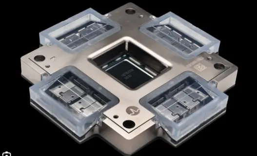
Source: Broadcom’s Bailly CPO ASIC
What is the Market Trajectory for the Photonics Industry?
The market trajectory of photonics is marked by significant advancements in integration density, material innovation, and the push for standardization.
Integration Density:
Photonic chips aim to combine more photonic and electronic components into smaller, cost-effective packages. Hybrid integration methods and chiplet architectures will enable this by 2030, with significant progress expected by 2040. There is a clear trend toward heterogeneous integration of light sources directly within photonic systems.
Interface Standardization:
Standardizing interfaces for photonics is critical for interoperability. The industry also needs testing standards that are cost-effective and thorough. Test equipment manufacturers will continue to invest in creating tools that can enable holistic cross-operations. This will reduce non-recurring engineering costs and shorten time to market.
Source: TFLN modulator
New Materials Beyond Silicon:
Researchers will continue to explore materials like III-V semiconductors, silicon nitride, hydex glass and graphene to overcome silicon’s limitations in light emission and detection. There has also been growing interest in TFLN (thin-film lithium niobate) and the experimental stage material called Perovskite.
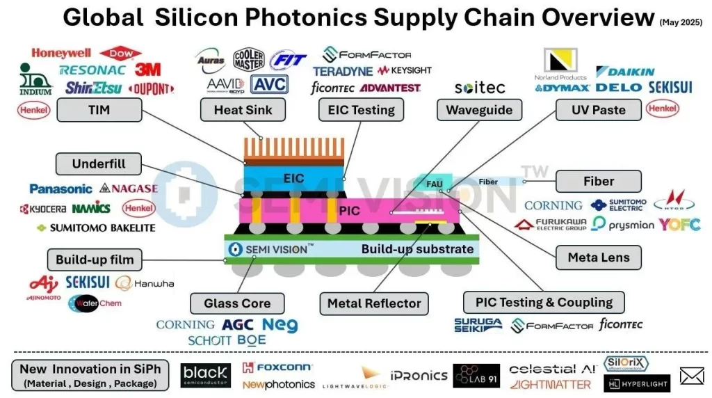
Optical-grade adhesives, capillary underfills, die-attach films and thermal interface materials will also be attracting significant interests from companies across the photonics ecosystem.
Thermal Management Innovations:
On-chip temperature control systems, like thermal tuners and localized cooling, are being developed to manage the thermal sensitivity of photonic components and ensure consistent performance.
Conclusion:
The photonics industry is advancing rapidly with innovations in integration density, materials, and standardization. By 2030, photonic chips will become more compact and cost-effective, with greater integration of light sources into photonic systems for enhanced efficiency.
Silicon photonics is already transforming data centers, but its potential extends to automotive safety, quantum computing, and augmented reality. Currently, growth is limited by the lack of accessible manufacturing facilities. Expanding open-access foundries is crucial to accelerate innovation and market progression.
With new materials like TFLN and Perovskite being explored, along with advancements in thermal management, photonics will continue to evolve. To stay competitive, companies need effective yield management. yieldwerx’s advanced tools provide real-time analysis and optimization, helping businesses streamline processes, enhance precision, and accelerate time to market.
Contact Us For a Free Consultation and Learn How yieldWerx Helps You Track, Test, and Improve PIC Performance.