In semiconductor manufacturing, precision is paramount, and ensuring that each chip layer aligns perfectly is crucial to achieving the desired product quality.
Enter closed-loop manufacturing—the backbone of modern quality control systems that enables real-time corrections to ensure consistent, high-quality output.
In this article, we’ll explore what closed-loop and feed-forward systems are, how they synergize to improve overlay accuracy, and which is the most critical yield limiter. In addition, we’ll discuss the challenges that semiconductor manufacturers face with closed-loop systems.
Let’s dive into the silent revolution that’s reshaping the way we think about quality checking procedures and predictive manufacturing.
Discover how yieldWerx can transform your semiconductor test data into smarter decisions and higher yields. Start your journey today by contacting us.
What is a Closed-Loop Control System?
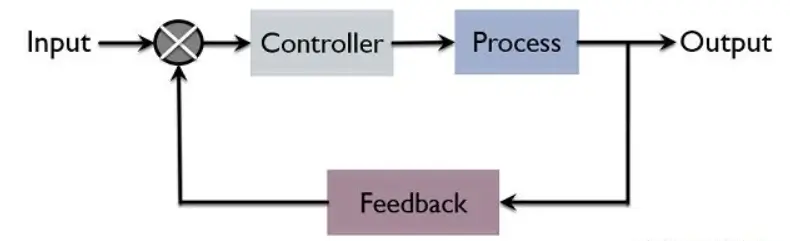
A closed-loop process control is an automated system that continuously monitors its output and compares it to a desired target. If there is any deviation, the system makes adjustments to correct it, ensuring the output stays within specified limits and identifying deviations promptly.
Key components include a setpoint (desired value), a sensor (measuring the output), a controller (comparing the actual output to the target), an actuator (making corrections), and feedback (sending the corrected output back to the controller). In short, deviations are corrected soon after they have occurred.
Thermostats and automotive cruise controls are some of the daily-life examples of closed-loop control systems.
What is a Feed Forward Control System?
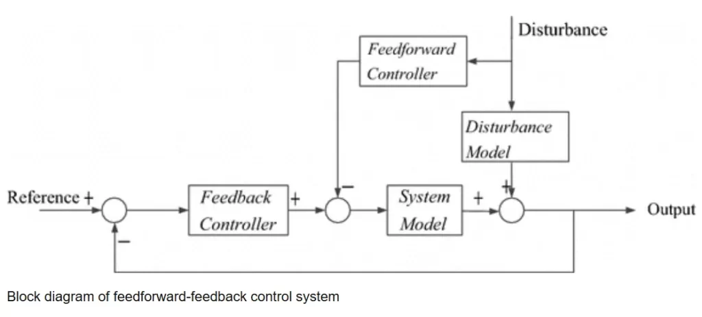
Feed-forward control is a proactive control system that aims to prevent deviations before they occur, rather than correcting them after the fact (as in closed-loop control). It uses predictive data or external measurements to anticipate changes and adjusts the process in advance to avoid potential errors.
In feed-forward control, the system monitors conditions that could affect the output, such as environmental factors, upstream processes, or system parameters, and makes adjustments to the process before the output is affected. This helps in minimizing errors and improving overall efficiency by acting on potential problems ahead of time, rather than waiting for feedback from the output.
Control System For Lithography
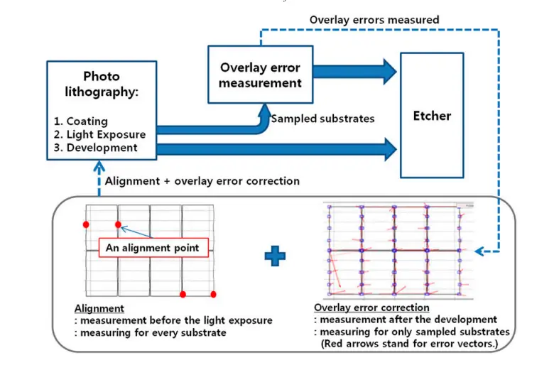
Overall overlay error control consists of the alignment and the overlay error correction.
Source: International Journal of Production Research
When today’s computer chips are built, dozens of very thin layers have to be lined-up on top of each other with nanometre-level accuracy. If one layer is even slightly shifted (“overlay error”), the tiny wires that make the circuit won’t connect properly and the chip can fail. Overlay control is all about ensuring precise alignment between the features on one mask layer with the one below.
Most factories already measure this error after a layer is printed and then tweak the machine for the next wafer. However, at the 10 nm scale and beyond that delay is often too late—the wafer is already mis-printed resulting in costly scrap and reduced yield.
What is Overlay Error?
Think of an animated flip-book: every drawing has to sit exactly on top of the previous one so the motion looks smooth. A modern integrated circuit is built the same way, but instead of pages there are 30-80 thin layers of patterns printed on a silicon wafer. Overlay control is the discipline of making sure each new pattern lands in precisely the right spot over the one below it.
At today’s nodes, interconnect wires are only a few dozen nanometres wide; the mis-alignment (“overlay error”) must stay below ~3-4 nm or the circuit won’t work. Bad overlay shorts or opens connections can turn good dies into scrap. Each additional nanometer of overlay error can cost fabrication facilities millions of dollars due to this yield degradation.
Automated Optical Inspection (AOI) systems assist in detecting these errors early, improving both precision and yield. Learn more about AOI data’s impact on semiconductor yield in our article.
What is Displacement?
Displacement specifically refers to the movement of the wafer’s surface caused by internal stresses, thermal gradients, or mechanical processes. It can occur in multiple directions (typically in the x, y, and z planes), leading to wafer warping or bowing. This shift can affect the alignment and pattern accuracy during processes like lithography, resulting in overlay errors.
What is warping?
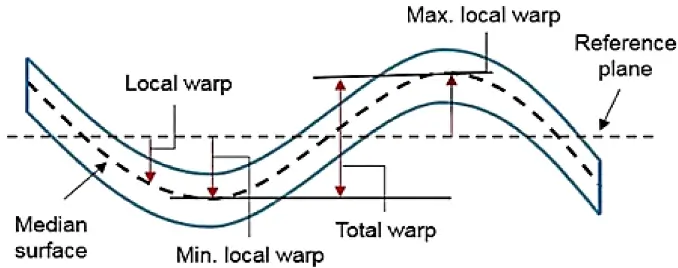
Wafer warping refers to the bending or deformation of materials. A daily-life example would be wood warping caused by unequal variations in the moisture content of different parts of a piece of wood. A semiconductor wafer’s surface experiences warping, caused by internal stresses, temperature fluctuations, or uneven material removal during manufacturing processes.
This warping can lead to alignment errors in processes like lithography. Common causes include film stress from thin film deposition, thermal expansion due to uneven heating or cooling, chemical mechanical planarization (CMP), and environmental factors such as temperature and humidity.
Improving Lithography Precision with Feed-Forward Controls and Wafer Displacement Data
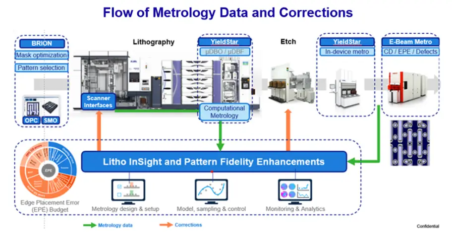
Feedforward and feedback of scanner and metrology data to correct for overlay errors. Source: ASML
Lithography is a critical process in semiconductor manufacturing, where patterns are transferred onto the wafer’s surface using light. As the industry moves toward smaller nodes (e.g., 10nm and below), achieving precise overlay between layers becomes increasingly difficult, as even tiny misalignments can lead to defects that affect the chip’s functionality.
To address this, feed-forward control systems are employed to proactively adjust the lithography process before exposure, minimizing errors and improving pattern fidelity. Unlike traditional closed-loop control, which corrects errors after they occur, feed-forward control anticipates potential issues and adjusts the process in real time based on predictive data.
One of the key factors affecting overlay accuracy is wafer surface displacement, which occurs due to process-induced stresses like thermal expansion, film stress, and CMP thinning. These displacements can cause the wafer to warp, leading to misalignment during the lithography process.
By using advanced measurement techniques like Coherent Gradient Sensing (CGS), manufacturers can capture high-density surface displacement data—up to 3 million data points per 300mm wafer. This data provides a precise map of how the wafer surface has shifted, indicating where potential overlay errors may have occurred.
With this displacement data, feed-forward controls can adjust overlay parameters before the lithography exposure. For example, if displacement data shows that a part of the wafer is warping due to thermal expansion, the system can pre-distort the lithography pattern to compensate for that misalignment, ensuring that the pattern lands exactly where it should when the exposure happens.
By combining wafer surface displacement measurements with feed-forward controls, manufacturers can significantly improve the precision and efficiency of the lithography process, leading to more accurate chip production and reduced rework.
Synergizing Closed-Loop and Feed-Forward Systems for Enhanced Quality Control
Manufacturers often synergize closed-loop and feed-forward systems to improve quality by combining the strengths of both approaches. By integrating both systems, manufacturers can achieve a more comprehensive approach to quality control.
Closed-loop systems handle real-time corrections, while feed-forward systems optimize the process in advance, reducing the risk of errors and improving overall product quality. Together, they enhance process stability, minimize rework, and boost yield, ensuring better consistency and efficiency in manufacturing.
Cost vs. Price: Evaluating Overlay Control Methods in Semiconductor Manufacturing
In the context of semiconductor processes, the cost and price of overlay control methods vary significantly. For feedback-only methods, fabs typically rely on existing overlay metrology tools, incurring costs related to extra rework cycles and possible yield loss, but the price is usually covered by current scanners and overlay tools, leading to a lower capital outlay. However, this comes with a greater risk of scrapped wafers.
In contrast, adopting feed-forward control, such as using CGS interferometers, involves costs related to buying and maintaining the CGS tool, integrating the data flow, and providing training. While the upfront cost is higher, feed-forward systems typically save on rework and improve yield, often offering a quick return on investment, especially at sub-10nm nodes.
Here, cost refers to the actual expenses the fab incurs to operate the equipment, while price is what the vendor charges. The fab then evaluates these costs against the expected yield improvements, which directly contribute to its overall profitability.
Challenges of Closed-Loop Systems in Semiconductor Manufacturing
While closed-loop systems provide valuable real-time corrections in semiconductor manufacturing, several challenges can hinder their effectiveness:
Latency in Response Time:
Closed-loop systems rely on feedback from the process to adjust, but this feedback often comes after a deviation occurs. This delay can be problematic, especially in high-precision processes like lithography, where even minor misalignments can result in defects.
Limited Data for Accurate Feedback:
Closed-loop systems rely on measurement tools to gather data, but in some cases, the data may not capture every variable influencing the process. In complex environments such as semiconductor fabrication, unmeasured factors can lead to inaccurate corrections.
Increased System Complexity:
Implementing a robust closed-loop system requires sophisticated measurement tools, algorithms, and constant recalibration, which can make the system more complex and costly to maintain.
Risk of Overcorrection:
If feedback is not properly analyzed or misinterpreted, closed-loop systems might overcorrect the process, introducing new errors or inconsistencies, which could compromise the final product quality.
Inability to Handle Unpredictable Events:
Closed-loop systems are primarily reactive, meaning they are not effective at preventing unforeseen events, such as sudden environmental changes or unexpected tool behavior.
Higher Equipment Wear:
Continuous feedback-driven adjustments may lead to increased wear on critical components in equipment, such as motors or sensors, leading to higher maintenance costs over time.
As a result of these challenges, closed-loop systems often need to be paired with feed-forward control, which can anticipate errors before they occur and prevent them, allowing for a more comprehensive control strategy that minimizes both reactive and proactive errors in semiconductor processes.
Conclusion
The combination of closed-loop and feed-forward systems revolutionizes semiconductor manufacturing by enhancing precision and efficiency. While closed-loop control corrects errors in real-time, feed-forward systems proactively prevent deviations, minimizing overlay errors and improving yield.
Despite the challenges of closed-loop systems, such as latency and increased complexity, integrating both systems offers a comprehensive solution for quality control, reducing rework and improving overall process stability. Although feed-forward controls come with higher initial costs, they deliver significant long-term benefits, making them essential for high-quality, cost-efficient manufacturing at advanced nodes. To enable the efficient application of both systems, manufacturers must have the capabilities to track real-time manufacturing deviations. Advanced yield management systems such as yieldWerx enables this type of precision with modules that enable quick feedback loops as well as predictive yield analytics.
Ultimately, the synergy between closed-loop and feed-forward systems is reshaping semiconductor manufacturing, driving greater consistency and higher quality while optimizing costs.
Contact Us For a Free Consultation and Learn How yieldWerx Helps You Extract Insights From Overlay Error Control Data.