Medical imaging has always been a race against time: delivering accurate diagnosis to patients with the speed modern healthcare demands. Traditionally, that meant large, immobile ultrasound machines tucked away in radiology departments, often forcing patients to wait days or weeks for the imaging needed to move forward with treatment. But in recent years, the industry has been moving toward something more agile and accessible—hand-held ultrasound devices. These pocket-sized tools are redefining how clinicians deliver point-of-care diagnostics by bringing imaging directly to the bedside, into emergency settings, and even into patients’ homes.
The rise of hand-held ultrasound is not just a story of portability. It’s a story of semiconductor innovation, photonics breakthroughs, and AI-driven intelligence converging to transform an industry that has long relied on bulky machines and specialized operators. With global revenues expected to exceed $500 million by 2026, hand-held ultrasound is redefining what’s possible when medical imaging breaks free from the confines of traditional hospital settings.

From Bulky Machines to Hand-Held Devices
For decades, ultrasound technology depended on piezoelectric transducers—bulky, crystal-based components that required complex wiring and limited frequency flexibility. Imaging was reliable, but the systems were expensive, heavy, and required trained technicians to operate. A patient needing a quick diagnostic scan had little choice but to be routed through hospital workflows that often delayed care.
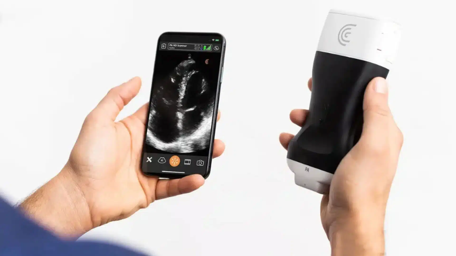
Today, the landscape looks dramatically different. Devices such as Butterfly Network’s CMUT-on-CMOS probes or GE’s Vscan Air are showing that imaging can be as portable as a stethoscope. A physician or nurse can slip a device into their pocket, connect it to a mobile phone, and capture detailed images on the spot. In emergency rooms, focused assessment with sonography for trauma (FAST) exams can be done immediately, even before the patient is wheeled inside. In home-care scenarios, a patient with a history of heart failure can be scanned for signs of fluid retention without ever setting foot in a clinic. These use cases illustrate how far the industry has come in making imaging more immediate, actionable, and patient-centered.
CMUT Ultrasound Chips: The Semiconductor Breakthrough

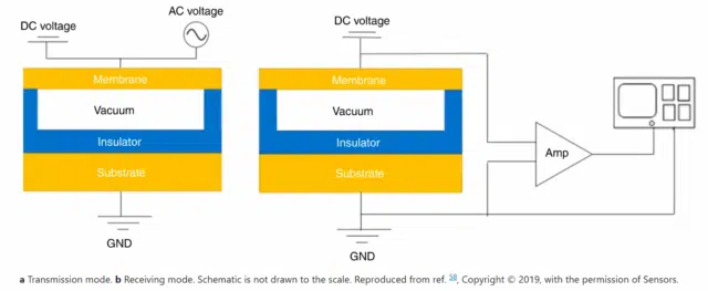
Overview of CMUT structure and different modes.
At the core of this transformation is the CMUT ultrasound chip (capacitive micromachined ultrasonic transducer). Unlike piezoelectric crystals, CMUTs can be fabricated directly on CMOS circuits, enabling thousands of tiny transducer elements to be integrated with their driving electronics on a single die. This shift mirrors the history of semiconductors, where integration unlocked scalability and cost efficiency.
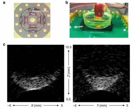
A CMUT-based device not only reduces the need for bulky cables but also allows for digital beamforming, multilevel pulsing, and on-chip data processing. In other words, the intelligence moves from the machine into the chip itself. This level of integration makes it possible to shrink devices down to hand-held form factors without sacrificing imaging quality. For semiconductor yield engineers and medical chip designers, the challenge now is ensuring these devices can be manufactured reliably at scale, with the precision required for medical compliance.

a) The schematic of IC for the dual-ring CMUT array. This IC includes receive IC, transmit IC, and the digital control circuitry. Schematic is not drawn to the scale. b) Experimental device of the CMUT for imaging ex vivo chicken heart phantom. c) Imaging results of the chicken heart phantom in XZ and YZ planes with 10 mm dimension size. Source: Nature.com
The Role of Photonics in Ultrasound
While CMUT chips are transforming the mechanics of ultrasound, photonics is opening a new frontier in sensitivity and speed. Photonics-based detectors, often built on crystal technologies, promise to push ultrasound into higher-resolution regimes while reducing latency in signal processing. Just as photonics has revolutionized data transmission in telecommunications, its role in photonics ultrasound could mean capturing deeper and clearer images in real time.
Photonics chips also hold the potential to improve thermal management and wavelength control, two of the most pressing challenges in miniaturized medical imaging devices. By combining light-based detection with advanced semiconductor packaging, engineers are exploring ways to make portable ultrasound more efficient, more durable, and better suited to continuous use in mobile healthcare environments. The implications extend beyond medicine, too: the same principles driving photonics ultrasound could apply to AR/VR devices, wearables, and consumer imaging technologies, further blurring the boundaries between healthcare and mainstream electronics.
AI-Guided Ultrasound: Lowering the Barrier to Use
Despite its promise, one of the biggest barriers to ultrasound adoption has always been the skill required to capture and interpret images. Even with portable devices, inexperienced users can struggle to position the probe correctly or make sense of what they are seeing. AI-guided ultrasound technology addresses this fundamental challenge.
Companies like Caption Health, Medo.AI, Pulsenmore, and ThinkSono are building AI systems that provide real-time guidance, labeling anatomy on the screen, and even offering preliminary interpretations. A nurse on rounds could use AI assistance to scan for vascular access. A midwife could assess fetal health in a rural clinic without waiting for a radiologist. In the future, patients themselves may be able to conduct basic scans at home, with AI providing confidence that images are usable and clinically relevant.
This democratization of expertise is what makes hand-held ultrasound so powerful. It’s not just that the device is smaller—it’s that AI enables healthcare providers to perform initial assessments outside of specialized radiology suites.
The Market Outlook: Adoption and Business Models
The global market for hand-held ultrasound is still in its early stages, but the growth trajectory is clear. According to Signify Research, the market grew by 30% in 2021 alone and is projected to continue its double-digit climb through 2026. Much of this adoption is being driven by new user groups such as primary care physicians, nurses, EMTs, and midwives—a sign that ultrasound is expanding beyond traditional hospital settings into more accessible clinical settings and scenarios..
Business models are also evolving. Vendors like Butterfly Network and Clarius are experimenting with subscription pricing, pairing affordable devices with paid digital services such as AI guidance, cloud storage, and tele-ultrasound. This shift reflects broader trends in healthcare technology, where hardware is often the entry point and recurring software services drive long-term value. Wireless devices, although currently a smaller share of the market, are expected to dominate in the future, untethering ultrasound from cables and making the experience more seamless for clinicians.
How Far Are We From Mass Adoption?

Source: NYTimes
While the trajectory is exciting, challenges remain. AI solutions must be validated rigorously to gain physician trust. Manufacturing CMUT and photonics chips at scale requires consistency and yield optimization across complex fabrication processes. And healthcare systems must adjust reimbursement and training models to accommodate new technologies.
Still, the direction is unmistakable. In the next decade, hand-held ultrasound powered by CMUT and photonics chips, guided by AI, and connected to the cloud will become a standard tool not just in hospitals but in clinics, ambulances, and homes. The result will be faster diagnoses, more accessible care, and a healthcare system that is more responsive to patient needs.
Conclusion: The Photonics Connection
At its heart, the future of ultrasound is a semiconductor and photonics story. Miniaturization, sensitivity, speed, and scalability are all challenges that photonics chips and CMUT ultrasound platforms are uniquely positioned to solve. For engineers and designers, this is an opportunity to redefine how medical imaging devices are built and deployed. For healthcare providers, it is a chance to deliver more precise, timely, and patient-friendly care.
At yieldWerx, we understand these challenges because they mirror the same complexities faced across the photonics and LED industry: wavelength control, miniaturization, and thermal management. But where we make the biggest impact for medical chip designers is at the level of manufacturing analytics and yield optimization.
Hand-held ultrasound chips require defect-free integration of MEMS, CMOS, and photonics structures. A single inconsistency in wavelength precision, thermal performance, or spectral uniformity can compromise device reliability—and in a regulated medical environment, that can mean product delays, compliance risks, and lost market opportunities.
This is where yieldWerx helps medical device innovators achieve scale without sacrificing quality. Our platform provides:
- Pixel-level analytics that detect brightness and spectral deviations across MEMS and photonic arrays, ensuring diagnostic images remain sharp and consistent.
- Advanced defect clustering and anomaly detection that highlight systematic manufacturing issues early, so chip designers can resolve them before they affect entire production runs.
- AI-powered commonality analysis that correlates yield loss across tools, processes, or lots, uncovering hidden connections that are otherwise invisible in complex fabrication environments.
- End-to-end lifecycle traceability, from wafer to packaged device, enabling medical chip makers to maintain full audit compliance and accelerate regulatory approval cycles.
- Automated dispositioning and scalability tools, allowing chip manufacturers to merge data across lots, product types, and process steps while applying rules tailored to their devices.
For medical chip designers, this means the ability to confidently bring CMUT and photonics ultrasound chips from the lab to mass production, while ensuring devices meet the uncompromising standards of both regulators and clinicians. In practice, that translates to faster product launches, higher yield stability, and lower risk of costly recalls or performance failures.
With yieldWerx analytics driving reliability at the chip level, and with photonics, semiconductors, and AI working together, the promise of photonics ultrasound is no longer on the horizon—it is rapidly becoming reality.
Ready to optimize your photonics and ultrasound chip manufacturing?
Contact us to get pixel-level analytics and accelerate scale-up while ensuring compliance.
Written by M. Rameez Arif, Content & Communication Specialist at yieldWerx.
Edited by Tina Shimizu, Content Strategist at yieldWerx.


