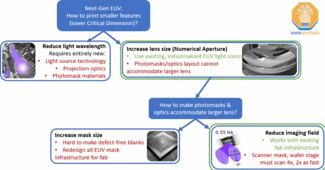
As chip designs push into 10nm, 7nm, and even 5nm nodes, traditional single-exposure lithography reaches its physical limits. The 193nm wavelength used in conventional lithography simply cannot resolve such small feature sizes in a single pass. This is where multipatterning lithography comes in.
Multipatterning allows chipmakers to print extremely dense patterns by breaking down a single critical layer into multiple exposures or self-aligned steps. By doing this, manufacturers can extend existing deep ultraviolet (DUV) lithography tools, avoiding the immediate need for a full transition to extreme ultraviolet (EUV) across all layers.
For manufacturers of high-performance logic devices, advanced memory, and feature-dense SoCs, multipatterning is not just an option—it is the only way to achieve the design fidelity required for next-generation chips.
Evolution of Multipatterning
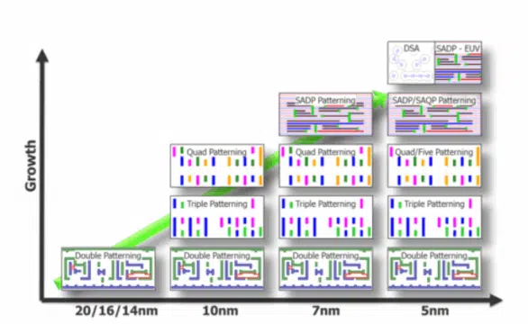
Growth of multi-patterning techniques by technology node
Multi-patterning in lithography originated as a solution to overcome the resolution limits of traditional single-exposure photolithography, becoming necessary as semiconductor features shrank below the capability of optical systems. The first demonstration of double patterning lithography occurred in 1983 by D.C. Flanders and N.N. Efremow.
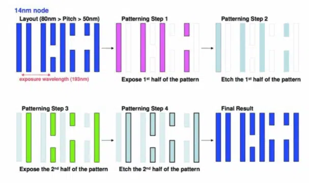
As semiconductor nodes reached around 20 nm and below, the smallest features could no longer be printed reliably with single exposures using 193 nm wavelength light. Early multi-patterning, also called pitch splitting or LELE (litho-etch-litho-etch), involved dividing the layout into separate masks, each exposed and etched independently, and then combined, enabling feature sizes smaller than the resolution limit of a single exposure.
However, this approach faced challenges due to misalignment between masks, limiting minimum pitch reduction. To improve precision, self-aligned techniques such as self-aligned double patterning (SADP) and self-aligned quadruple patterning (SAQP) were later developed, which use spacer technology to define features with higher alignment accuracy.
Multi-patterning became widely adopted in the 2000s and 2010s for critical semiconductor nodes like 14 nm, 10 nm, and 7 nm, particularly in NAND flash and DRAM manufacturing, extending the usefulness of 193 nm lithography while extreme ultraviolet (EUV) lithography was still emerging.
Even with EUV, multi-patterning remains essential for many layers due to throughput and defectivity challenges. This technology has been critical for continuing feature scaling and Moore’s Law in advanced integrated circuit manufacturing.
Understanding Double Patterning and Quadruple Patterning
When we talk about multipatterning, two techniques dominate: double patterning and quadruple patterning.
Double Patterning: The Bridge to 10nm
Source: Cadence
Double patterning, also called litho-etch-litho-etch (LELE) process, splits a single critical layer into two separate masks, each exposed and etched sequentially. By combining these two exposures, manufacturers effectively double the achievable pattern density. This technique became essential at the 20nm and 14nm nodes and continued to be used even down to 10nm.
Quadruple Patterning: Critical at 7nm and Below
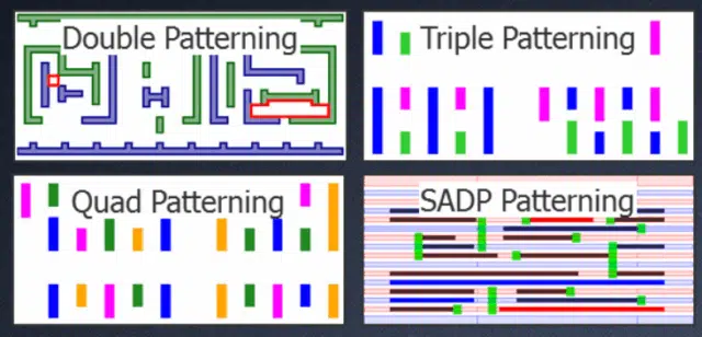
At 7nm and beyond, even double patterning is not enough. Quadruple patterning takes the process further by using additional spacer-based patterning steps to quadruple the effective resolution. This technique is commonly deployed in high-density layers like SRAM bitcells and advanced interconnect layers.
The move from double to quadruple patterning doesn’t just add cost and complexity—it fundamentally changes how engineers must approach yield management. Each additional patterning step creates a new potential source of variation and defects.
Why Multipatterning Makes Defect Detection More Difficult
Source: SemiAnalysis
With every additional patterning step, the number of variables affecting yield multiplies. These are some of the biggest pain points for semiconductor manufacturers operating at 10nm and 7nm:
1. Multiple Exposure Sources of Variation
Each exposure in multipatterning introduces potential overlay errors, line-edge roughness, and critical dimension variations. These variations may not cause immediate defects but can stack across patterning steps, ultimately creating systematic yield loss. Therefore, increasingly stricter overlay control is needed.
2. Coloring and Decomposition
Every IC design must be decomposed into multiple masks through a process known as layout coloring. This ensures that patterns can be accurately manufactured within lithographic limits.
Depending on the methodology, this can follow a colorless flow, where decomposition is fully automated; a partial coloring flow, where designers manually assign colors to critical features to control variation; or a full coloring flow, where every feature is explicitly assigned to a specific mask.
Additionally, color balancing across masks is crucial, as uneven mask densities can lead to lithography and etch variations, impacting critical dimensions and overall yield.
2. Mask-to-Mask Interactions
Defects are no longer isolated to a single mask. A misalignment between two masks or a spacer defect during quadruple patterning can create complex, hard-to-trace defect signatures.
3. Increased Defect Ambiguity
Traditional inspection methods often generate false positives when dealing with multipatterning. Non-critical variations in one mask may be mistakenly flagged as defects, flooding yield teams with data that is difficult to prioritize.
4. Slower Root-Cause Analysis
When one defect signature may involve two, three, or even four different patterning steps, manual defect attribution becomes extremely time-consuming. Yield ramp slows down as teams spend weeks chasing down the source of yield loss.
5. Increased Manufacturing Costs
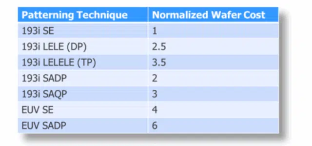
Normalized wafer cost adder for different patterning schemes Source: Siemens
Multi-patterning demands additional masks and multiple lithography and etching steps for each layer, significantly increasing the cost per wafer. Each new mask adds design, inspection, and manufacturing overhead. These extra process steps also slow wafer throughput, extending cycle times and potentially delaying time-to-market for new products.
How Yield Management Tools Help with Multipatterning Defects
As multi-patterning designs grow in complexity, each process step generates vast amounts of data, making it exponentially harder to trace the exact genealogy and origin of defects.This is where a modern yield management solution like yieldWerx comes in.
Pattern-Centric Defect Analysis
yieldWerx allows engineers to correlate defects directly with individual lithography steps. For example, if a defect pattern only shows up when Mask B is used in double patterning, yieldWerx’ analytics engine highlights that correlation instantly, allowing engineers to focus their efforts where they matter most.
Overlay-Aware Defect Detection
Overlay errors between masks are one of the most common yield limiters in multipatterning. It integrates overlay metrology data with test results, giving engineers a direct link between alignment issues and yield loss.
Good Die, Bad Neighborhood (GDBN) Identification
Multipatterning defects often create localized “hotspots” of failure across a wafer. yieldWerx’ GDBN detection capabilities quickly identify these systematic defect clusters and provide insights into whether they stem from lithographic steps or downstream processes.
Automated Root-Cause Correlation
Instead of manually correlating test data with fab data, it automates this process. Engineers can drill down from high-level yield dashboards into specific wafers, masks, and even die-level defect signatures—all within a single platform.
How YieldWerx Defect Detection Excels in Multipatterning Environments
yieldWerx is built to handle the complexity of multipatterning nodes. Some of its most powerful capabilities include:
- Layer-to-Layer Defect Correlation: Link defect signatures across masks to pinpoint root causes in complex double or quadruple patterning flows.
- Advanced Visualization Tools: Wafer maps, defect clustering overlays, and mask correlation charts give engineers the context they need to act fast.
- Real-Time Defect Monitoring: Quickly detect systematic issues before they propagate through subsequent process steps.
- Seamless Integration: yieldWerx works with fab data, test data, and metrology data to deliver a unified defect analytics environment.
Conclusion: Turning Multipatterning Complexity into Yield Opportunity
Multipatterning is no longer an advanced technique for a few specialized layers—it is the foundation of modern chip manufacturing at 10nm, 7nm, and beyond. But with this added complexity comes a critical challenge: defect detection.
By adopting yieldWerx, semiconductor manufacturers can:
- Identify lithography-related defect patterns faster.
- Correlate defects with specific masks or spacer steps.
- Automate root-cause analysis and reduce debug time.
- Accelerate yield ramp in the face of increasing design complexity.
The future of defect detection in multipatterning environments will belong to companies that embrace data-driven yield management. yieldWerx provides the tools to make this transition not just possible, but profitable.
Ready to simplify defect detection in multipatterning environments?
Book a Demo today and see how our defect detection platform turns 7nm and 5nm yield complexity into actionable insights.
Written by M. Rameez Arif, Content & Communication Specialist at yieldWerx.
Edited by Tina Shimizu, Content Strategist at yieldWerx.
References:
- Cost model for low- & high-NA EUV, Feature Fidelity, Technical Challenges
- Will EUV Kill Multi-Patterning?
- The History of Lithography, Part 2: From Double-Patterning to EUV
- Multiple Patterning
- Generation of <50 nm period gratings using edge defined techniques
- Changes and Challenges Abound in Multi-patterning Lithography