Why Shift Left Matters Now in Semiconductors
Every semiconductor engineer understands the cost-of-change curve: the later a problem is discovered, the more expensive it becomes to fix. What has changed is the slope of that curve.
Advanced nodes now mean that each downstream step carries a far greater cost penalty when discovered late. In addition, yield loss is rarely caused by a single catastrophic defect. Instead, it is usually the result of small design sensitivities, process interactions, and subtle variations that compound over time. They often become visible only after expensive manufacturing steps have already occurred.
Historically, the industry has relied on a reactive model:
manufacture → test → analyze → debug.
But according to industry analyses published by organizations such as SEMI and McKinsey, the cost of yield loss increases exponentially as a defect progresses further downstream.
This is the core motivation behind shift left testing methodology in semiconductor manufacturing:
Moving yield intelligence, correlation, and decision-making earlier in the lifecycle, where action is still affordable and effective.
What “Shift Left” Means for Semiconductor Yield Management
In semiconductor manufacturing, shift left is not about earlier testing alone; it is about enabling earlier learning and decision-making.
A shift-left yield strategy focuses on:
- Identifying yield risks before physical manufacturing amplifies them
- Correlating design intent with process behavior early
- Detecting systematic issues at wafer sort or even pre-silicon stages
- Preventing low-quality devices from consuming downstream resources
In practice, this means extending yield analysis beyond the final test and embedding it across:
- Design revisions and mask changes
- Process steps and lot genealogy
- Wafer-level, die-level, and site-level test data
- Assembly, packaging, and system-level results
This upstream visibility enables manufacturers to act on signals rather than symptoms.
Why Test-Only Yield Models Are No Longer Sufficient
For many years, the final electrical test served as the primary gatekeeper for quality. That approach worked when devices were monolithic, and failure modes were relatively isolated.
Today’s products are fundamentally different.
Advanced Nodes and Process Sensitivity
At leading-edge nodes, even minor variations in lithography, stress, or voltage margins can create parametric fallout. Process variability increasingly dominates yield behavior at advanced geometries—often in ways that are difficult to diagnose late in the flow.
Chiplets and Heterogeneous Integration
Companies like Intel and AMD have publicly discussed the challenges of chiplet-based architectures. In these designs, yield is no longer determined by a single die but by the interaction of multiple dies, interfaces, and packaging technologies.
A failure detected after full package assembly may originate from:
- One marginal die
- An interface mismatch
- Thermal or mechanical stress introduced during assembly
A test-only yield approach struggles to untangle these dependencies.
The Economics of Late Discovery: Why Shifting Left Saves Money

The financial argument for shift left is especially strong in modern semiconductor manufacturing.
Packaging Cost Escalation
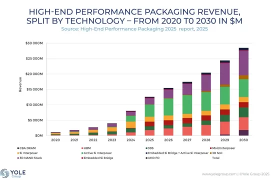
Advanced packaging technologies—such as silicon interposers, fan-out wafer-level packaging, and 3D stacking—add high cost per unit. Public disclosures from TSMC and ecosystem partners consistently show that packaging is now one of the fastest-growing cost components in the overall manufacturing flow.
Scrapping a device after advanced packaging can cost multiples of what early disqualification would have.
Test Time and Resource Consumption
Beyond packaging, late failures consume:
- Additional tester time
- Burn-in and reliability testing resources
- Engineering debug effort
- Capacity that could have been used for good die
Shift-left yield strategies aim to filter or correct issues earlier, preserving both margin and capacity.
From Yield Analysis to Lifecycle Intelligence
True shift-left adoption requires more than moving a single checkpoint earlier. It requires connecting data across the entire product lifecycle.
This is where the industry’s focus on digital thread and digital twin architectures becomes essential.
When design data, process conditions, and test outcomes are unified:
- Yield issues can be traced to their true origin
- Debug cycles shrink dramatically
- Learning from one product or node can be reused on the next
Platforms such as yieldWerx are built around this principle—treating yield not as an isolated test function, but as a continuous intelligence layer spanning design through system-level validation.
Digital Twin and Digital Thread in Practice

Shift-left manufacturing depends on generating reliable insight before failures manifest in silicon. Digital twins support this objective by allowing teams to explore how design decisions, process conditions, and manufacturing variability interact earlier in the lifecycle, when corrective action is still feasible.
Leading semiconductor manufacturers increasingly rely on digital twins to understand and predict how complex design, process, and manufacturing decisions interact long before failures appear in silicon. For example, a design that meets performance targets in simulation may prove highly sensitive to line-edge roughness or local stress effects at advanced nodes, increasing the likelihood of parametric fallout later in manufacturing.
Digital twins also enable a more proactive treatment of process variation. Rather than viewing variation as random noise, manufacturers can model how shifts in lithography focus, implant conditions, or metal thickness reshape parametric distributions across wafers and lots. This allows teams to anticipate which combinations are most likely to drive yield loss and prioritize mitigation earlier in development.
While digital twins provide predictive insight, their true value is unlocked when combined with a digital thread. The digital thread ensures that insights discovered at one stage of the lifecycle remain visible and actionable at subsequent stages. For instance, spatial anomalies detected during wafer sort—such as edge-related parametric shifts or reticle-level patterns—can be automatically traced to assembly outcomes or final test behavior. This traceability allows teams to recognize recurring failure signatures, validate hypotheses faster, and avoid rediscovering the same issues at each new stage.
Real Benefits Of Shift Left Testing Observed Across the Industry

Manufacturers adopting shift-left yield strategies consistently report:
- Faster root-cause isolation during yield excursions
- More predictable yield ramps for new products
- Reduced scrap and rework at advanced packaging stages therefore promoting sustainability goals.
- Stronger collaboration between design, process, and test teams
In high-volume manufacturing, even small improvements in early yield insight can translate into millions of dollars in savings over a product’s lifetime.
Challenges to Implementing Shift Left Test Strategy
Despite its clear benefits, implementing a shift-left test strategy is not trivial. One of the biggest challenges is fragmented data ownership across design, process, test, and assembly teams, each operating with different tools, data models, and priorities.
The chip industry is full of legacy equipment. Such yield and test systems often exacerbate this issue, as they were not designed to scale with today’s data volumes or to handle the complexity of spatial, parametric, and contextual data generated by advanced devices and packaging technologies.
Organizational barriers can be just as significant as technical ones. Shifting yield left requires cross-functional transparency and shared accountability—conditions that are difficult to achieve in environments where yield responsibility is confined to late-stage test or manufacturing.
In addition, correlating electrical results with spatial patterns, process conditions, and design intent remains a complex analytical challenge. Overcoming these obstacles requires more than incremental improvements; it demands modern, scalable data platforms paired with a cultural shift toward lifecycle-wide ownership of yield outcomes.
The Future of Shift Left in Semiconductors

Looking forward, shift-left yield management will increasingly be driven by:
- AI and machine learning–based predictive yield models
- Virtual yield ramps before volume production
- Automated correlation across design, process, and test domains
- Deeper integration with system-level and field data
As device complexity continues to rise, competitive advantage will belong to manufacturers who can learn earlier and act faster than yield issues can propagate.
yieldWerx: Operationalizing Shift-Left Yield Intelligence
To enable a true shift-left approach, yieldWerx re-architects yield intelligence by expanding analysis across the entire semiconductor lifecycle, breaking away from isolated, test-only workflows.
yieldWerx expands visibility across:
- Design Data ↔ Process Data ↔ Test Data ↔ Assembly ↔ System-Level
- Complete traceability and automated lot dispositioning
- Multi-modal detection methods, AI-driven PAT++ with zonal analytics
- End-to-end digital intelligence across the product lifecycle
This approach transforms test and yield engineering from a reactive, post-test activity into a predictive, connected discipline.
When design models, mask revisions, process data, and test data exist within a unified ecosystem:
- Excursions are isolated at their true point of origin
- Debug cycles shorten dramatically
- Failures can be correlated by IP block, mask layer, reticle, or design revision
- Teams gain clear insight into the true drivers of yield, reliability, and quality
As a result, yieldWerx customers often achieve 5–10× faster root-cause analysis—not because they are testing more, but because they are connecting more.
At the platform level, yieldWerx is one of the few test and yield management solutions that:
- Links design artifacts, engineering changes, and mask revisions directly to yield and reliability signals
- Enables a closed-loop learning environment across design, fabrication, assembly, and test
- Provides complete lifecycle traceability from concept → tapeout → wafer → package → final system
Taken together, these capabilities position yieldWerx as a foundational intelligence layer within the manufacturing ecosystem. Companies choose yieldWerx because it:
- Supports diverse data domains including electrical, optical, photonics, sensors, chiplets, and SLT
- Bridges silos across design, process, test, assembly, and system engineering
- Scales globally across factories and suppliers
- Drives automation, root-cause acceleration, and manufacturing intelligence
- Supports the full lifecycle from NPI through ramp to high-volume production
Ready to move yield intelligence upstream?
If you’re modernizing your manufacturing data infrastructure or building next-generation devices, now is the time to adopt a connected, shift-left testing approach to yield management. Explore how yieldWerx can help you turn lifecycle data into earlier insight and faster action.


