Semiconductor yield engineers handle hundreds of test records every day, from wafer sort to final test. Yet much of this valuable information remains trapped in disparate files, formats, and spreadsheets. More than 80% of the data generated across the semiconductor supply chain, from design and manufacturing to field operations, is never analyzed. Data cleaning alone consumes over half of the total time and effort spent on analysis, leaving engineers with less time to extract real insights from non-standard test data.Those hours are often eaten up by repetitive manual processes, not meaningful investigation.
The exponentially increasing amount of data, the storage of data, and the general poor quality of data is a hidden crisis that costs manufacturers billions every year. In the United States alone, companies lose an estimated $3.1 trillion annually due to inaccurate, incomplete, or duplicate data. For semiconductor manufacturers, the impact is even more pronounced—where precision and data integrity directly affect yield performance and profitability.
Just as chips are made in spotless clean rooms, we also need clean, error-free testing data. In this post we explore how manual data manipulation has become a silent productivity killer in semiconductor testing. We’ll look at the challenges engineers face when working across multiple testers, fabs, and global teams and share how adopting automated, centralized data manipulation tools like yieldWerx can turn scattered data into actionable yield insights.
It’s time to move beyond manual processes. Automate your data manipulation with yieldWerx today.
What Is Data Manipulation in Semiconductor Testing?
At its simplest, data manipulation means preparing data (aligning, transforming, cleaning, or reformatting) to make it usable for analysis. In semiconductor testing, it refers to how engineers manipulate data from STDF (Standard Test Data Format), ATDF, KLARF, or other data file formats to extract yield, bin, and parametric insights.
When test data arrives from different testers or fabs, it rarely follows a single schema. Test names might differ (“I_DD” vs “IDD”), numeric precision can vary, and unit mismatches are common. Engineers then have to manually manipulate data—renaming columns, aligning parameters, and validating values—before they can even begin yield analysis.
What Is the Difference Between Manual, Semi-Automated, and Fully Automated Data Manipulation?
In manual data manipulation, engineers handle every step from managing test data input, cleaning it in spreadsheets, and formatting it for analysis. Such manual processes are slow and error-prone.
In semi-automated data manipulation, scripts or basic data management tools (like Python, R) assist with cleaning and merging, but engineers still configure and validate each run.
In fully automated data manipulation, data flows directly from testers to centralized systems where it’s standardized and prepared automatically, giving engineers instant access to clean, analysis-ready datasets. Such automated tools are the choice of all large-scale semiconductor companies.
Learn more about the complete test data manipulation process at the link below:
Complete Guide to Test Data Manipulation in Semiconductor Manufacturing
What Are the Challenges with Manual Data Manipulation?

Manual data handling in semiconductor analytics may seem manageable using Excel spreadsheets, but it quickly becomes unscalable, even for startups. Each lot, wafer, and die can produce millions of data points across multiple testers and product lines, turning integration into a constant struggle.
Different testers like Advantest, Teradyne, or Emerson Electric output STDF or proprietary files with varying field names and formats. One site may label a field “FAIL_BIN,” another “FBIN.” Without a unified schema, engineers must manually clean, re-map, and merge data from multiple legacy testing sources and fabs, wasting hours on formatting instead of analysis.
Relying on spreadsheets and ad-hoc scripts introduces frequent human errors like misplaced decimals, truncated fields, or duplicated entries that can distort yield metrics. These tools lack version control and audit trails, making it nearly impossible to trace mistakes or ensure consistency.
When different fabs or teams follow their own data handling conventions, organizations lose the ability to build a unified view of test performance leading to many missed opportunities. Every new product, tester, or facility adds another layer of manual alignment, slowing decisions and reducing confidence in the results.
The Hidden Cost of Spreadsheets and Local Scripts
Spreadsheets and local scripts offer short-term convenience but create long-term inefficiency. They lack standardized schemas, validation rules, and version control. Multiple engineers often edit copies of the same sheet, leading to high error rates and lost traceability. Spreadsheets also fail to handle large datasets effectively, making them unsuitable for modern semiconductor test volumes.
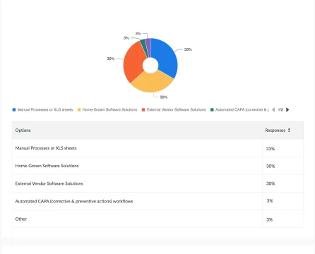
Manual repetition compounds the problem. Each wafer or lot requires the same cleansing and transformation steps, delaying reporting cycles and masking early warning signals. Internal estimates from several semiconductor firms show that manual data preparation can consume up to 30% of total test engineering time. When scaled across global operations, these inefficiencies can translate into hundreds of thousands of dollars in wasted effort annually.In a study conducted by yieldWerx, it was shown that 33% of top semiconductor companies still use manual processes and Excel spreadsheets to track data.
The Strategic Limitations of Manual Data Manipulation
Beyond the operational burden, manual data manipulation limits strategic agility. By the time data is ready for review, process conditions may have already changed. Organizations miss narrow windows for corrective action when they rely solely on manual workflows. Missing outliers or misaligned identifiers can trigger false corrective actions or hide systemic failures. While spreadsheets seem inexpensive, their hidden costs such as lost time, lack of traceability, and inconsistent analytics make them unsustainable in data-driven semiconductor environments.
What Are the Challenges with Semi-automated Data Manipulation?
Semi-automated data manipulation offers some efficiency compared to manual methods, but it still faces significant challenges that limit scalability and reliability.
Engineers must continuously maintain and update Python scripts, especially when test formats or data structures change. Each tester, fab, or product line might output slightly different file types or field names, forcing constant adjustments to parsing logic.
Error handling remains manual. If a script fails or encounters missing data, engineers need to debug and rerun it. This interrupts workflows and introduces delays.
Data validation and consistency checks are also weak in semi-automated setups. Since scripts often lack built-in standardization rules, they can still output inconsistent or incomplete datasets that require human review.
Finally, scalability becomes a bottleneck. What works for one or two testers may fail across global teams. Without centralized monitoring or scheduling, engineers spend more time managing automation than benefiting from it.
In short, semi-automated data manipulation reduces some effort but still suffers from fragility, maintenance overhead, and limited scalability compared to fully automated pipelines.
Automated and Centralized Data Manipulation: A Smarter Path
There is a growing trend amongst semiconductor companies to adopt specialized data manipulation software to automate test data cleansing, validation, and transformation at scale. The primary reason is that traditional manual or semi-automated workflows simply can no longer keep pace with the volume, variety and velocity of today’s test data.
Organizations gain data consistency and quality control by deploying centralized automated data manipulation tools. These systems enforce standard rules for test naming, units, limits and output formats across fabs and testers, which greatly reduces human error rate and response times. Meanwhile, these platforms support scalability across testers and fabs, seamlessly parsing multiple formats and proprietary outputs, and consolidating them into a single unified repository. Deployment and operational cost are easily justified over the long run mainly due to the number of work-hours saved.
Engineers get real-time data access rather than waiting days or weeks for manual consolidation. Clean and standardized datasets are immediately available for yield analysis, root-cause investigations or dashboards. This shift enables reduced engineering overhead: repetitive and error-prone tasks like manual cleanup, merging and validation are eliminated, freeing teams to work on higher-value activities such as modelling, optimisation or predictive analytics.
Finally, centralised and automated manipulation ensures auditability and traceability. Every transformation step is logged, changes are version-controlled, and data lineage is preserved which supports compliance, quality assurance and robust decision-making.
Why yieldWerx is the Smarter Choice for Data Manipulation
To overcome the challenges of manual and semi-automated workflows, many semiconductor teams are turning to yieldWerx, a modern platform designed for automated and centralized data manipulation achieving high levels of customer satisfaction.
Unlike traditional tools that require complex setup and rigid infrastructure, yieldWerx is easy to deploy and can be customize to meet each customer’s requirements. Test data can be loaded directly by internal teams or with the support of yieldWerx’s experienced development group, ensuring a smooth and efficient onboarding process. While the initial investment may seem like a hurdle, the long-term cost efficiency is undeniable.
yieldWerx’s modular architecture offers flexibility for companies of all sizes. Large enterprises can integrate the platform across multiple fabs and test sites, while smaller organizations can begin with select modules and scale as operations expand. The platform supports a wide range of data formats—including STDF, ATDF, Klarf, CSV, and proprietary outputs—through custom-built parsers that consolidate files into a single, standardized repository for faster analysis and decision-making.
With yieldWerx, engineering teams gain real-time access to clean, validated, and standardized datasets, eliminating hours of repetitive data preparation. Built-in audit trails and version control deliver full traceability and ensure compliance with the strict standards required in healthcare, defense, and automotive sectors.
In short, yieldWerx combines speed, accuracy, and flexibility in a single solution, helping semiconductor organizations—from startups to global players—transform their data manipulation processes and unlock actionable insights faster.
Let your yield engineers focus on the actual root cause analysis and not data cleanup. See yieldWerx in action to learn more.
Written by M. Rameez Arif, Content & Communication Specialist at yieldWerx.
Edited by Tina Shimizu, Content Strategist at yieldWerx.