Ending The Bandwidth Bottleneck in Modern Computing with Co-Packaged Optics (CPO)
The exponential growth of high-quality video streaming, AI/ML workloads, IoT, and cloud computing has created unprecedented demands for increased bandwidth by 23% year-over-year, with data centers facing rising power demands. Simultaneously, electrical interconnects have reached physical limits on speed, efficiency, and latency.
Traditional copper-based interconnects are struggling to deliver the signal reach, power efficiency and speed that modern computing demands.. Co-Packaged Optics (CPO) is emerging as the semiconductor industry’s answer to this bandwidth bottleneck.
By integrating optical components directly with compute or switch chips, CPO promises higher bandwidth, lower latency, and dramatically improved energy efficiency.
This article explores what Co-Packaged Optics (CPO) is, why chiplet integration is crucial, and how photonics can redefine high-bandwidth computing.
What are Co-Packaged Optics (CPO)?
Co-Packaged Optics (CPO) refers to the integration of optical input/output (OIO) directly alongside ASICs or switches within a single advanced package. This eliminates long copper traces and brings fiber connectivity closer to the logic die, eliminating electrical interference and crosstalk.
CPO differs from traditional optical approaches such as pluggable optics or near-package optics (NPO). In pluggables, optical transceivers connect externally through electrical interfaces, which adds latency and power overhead. NPO brings optics closer to the package but still keeps them separate. CPO fully merges the optical and electrical domains within one integrated system.
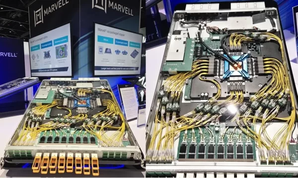
Leading companies are already implementing CPO to meet these demands. In Nvidia’s Spectrum-X and Quantum switches, CPO enables high-speed optical links optimized for AI data centers. NVIDIA also plans to adopt CPO in its GB300 series and future Rubin architecture, replacing electrical NVLink with optical interconnects.
The Limitations of Pluggable Optics
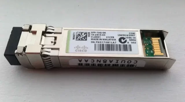
Pluggable optics are modular optical transceivers that connect to switches or servers via electrical interfaces. They convert electrical signals into optical signals for high-speed data transmission across fiber networks. Widely used in data centers and cloud infrastructure, pluggables have evolved from 100G to 400G, 800G, and 1.6T, enabling faster communication between chips and across racks. However, they are reaching their physical and thermal limits as network capacities scale to 6.4T and 12.8T.
Here are some of the reasons for that.
The Compute and I/O Imbalance
Over the past two decades, silicon chip performance has skyrocketed thanks to Moore’s Law and companies like TSMC introducing smaller nodes, but optical input/output (I/O) and memory technologies haven’t kept pace, resulting in a growing bandwidth bottleneck between compute and I/O.
What is The SerDes Power Challenge For CPOs?
Why does optical I/O lag behind?
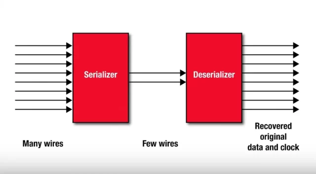
A major reason is the SerDes—short for serializer/deserializer. Switch chips send data in parallel across many lanes at lower speeds, but optical fibers can only carry data serially, one stream at a time. The SerDes is responsible for converting these parallel electrical signals into a serial stream for transmission, and then converting them back on the receiving end.
You can think of it like an airport gate. Passengers arrive from multiple directions, and the gate agent (the serializer) organizes them into a single line that boards the plane in order. When they reach their destination, another agent (the deserializer) helps them disperse into multiple exits again.
At extremely high speeds—tens or hundreds of gigabits per second—electrical signals traveling through copper begin to degrade, causing integrity issues. To correct this, the SerDes uses advanced signal processing techniques or boosts weakened signals through equalization. Both methods consume a significant amount of power, making SerDes one of the fastest-growing power consumers in data center systems.
Huawei once estimated that in its 28-nanometer switch, SerDes circuits accounted for around 10–15% of the chip’s total area and power. A decade later, that share has more than doubled.

What Are Some of the Thermal and Spatial Inefficiencies Associated With CPOs?
Pluggable optics also create thermal and spatial challenges, which are additional reasons for adopting CPOs. Traditional pluggable optics sit on switch faceplates, which restrict airflow and limit how densely systems can be built. By moving optical I/O inside the package with CPO, it can then free up space and improve cooling, allowing for denser, higher-bandwidth systems. While CPO presents its own engineering challenges, it offers a clear path forward for energy-efficient, scalable, high-speed computing.
What Is The Role of Chiplets and Advanced Packaging For CPOs?
To overcome the power and thermal challenges with traditional pluggables, Co-Packaged Optics (CPO) relies on chiplet-based designs, which are central to the CPO revolution. Instead of fabricating a single large die, manufacturers build smaller chiplets that integrate specific functions such as compute, memory, or photonics.
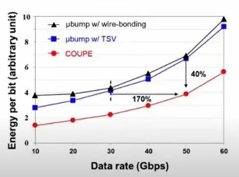
Advanced packaging technologies like TSMC’s COUPE platform and Intel’s Foveros or EMIB make it possible to connect these heterogeneous dies within one system. This approach supports modular upgrades, reduces fabrication costs, and improves design flexibility. TSMC claimed that COUPE improved the photonic engine’s power consumption by 40% and raised its speed by 170% compared to other ways of connecting.
By integrating photonic chiplets alongside logic and memory dies, CPO systems can scale more efficiently while maintaining superior power and thermal characteristics.
What Are the Challenges of Co-Packaged Optics?
The semiconductor industry is traditionally conservative by nature, relying on proven technologies for stability and reliability. Faceplate pluggable transceivers have been the standard for years—they’re affordable, easy to replace, and supported by well-established standards that offer plenty of vendor options. Convincing customers to move away from such a proven and familiar technology will be challenging.
Vendor Lock-in
Without a doubt, CPOs reduce sourcing flexibility as optics and electronics are tightly coupled. Datacenter management firms may feel uncomfortable with the amount of dependency on single vendor solutions that can limit scalability and interchangeability.
Manufacturability and Cost
CPO is still expensive compared to pluggables and needs better yields and testing methods. As production scales, costs should decrease, but consistent quality in a multivendor ecosystem remains a challenge.
Thermal Management
Integrating photonics inside ASIC packages creates significant thermal challenges. Heat from electrical and optical components can cause thermal crosstalk, affecting both performance and reliability. Liquid cooling and advanced thermal modeling are essential.
Signal and Power Integrity
CPOs demand precise electrical-photonic simulations to ensure signal and power integrity. Parasitic effects at the packaging level must be carefully modeled to maintain high-speed performance and minimize losses.
Coupling and Fiber Alignment
Efficient optical coupling between fibers and photonic chips is complex due to scale mismatches. Passive or active alignment and innovative approaches like grating-based coupling or V-grooves are used to minimize light losses.
Scalability and Beachfront Limitations
Bandwidth density along the chip’s edge (beachfront) is limited by fiber spacing. Managing thousands of fiber connections without increasing substrate size requires creative packaging and optical coupling strategies.
Reliability Proof and Industry Adoption
Although CPO eliminates some common failure points, its reliability must still be proven through large-scale, long-term deployments. Industry players are running pilot tests to validate both costs and yields.
What Is The Role of Advanced Test Data Analytics For CPO Yield Management?
Advanced test data analytics plays a critical role in dealing with the challenges mentioned above to improve yield and reliability in Co-Packaged Optics (CPOs). As electrical and optical components sit side by side, even small variations in wafer fabrication, photonic alignment, or thermal behavior can affect overall performance. Traditional silicon testing methods often miss these subtle interactions, which makes advanced optical analytics essential.
By applying AI-driven anomaly detection, and multidimensional data correlation, engineers can quickly find patterns, trace the root causes of defects, and predict potential yield issues before they impact production. Analyzing data from wafer probe to final module testing helps teams link electrical and optical performance, uncovering process dependencies that manual inspections overlook. Real-time analytics also supports adaptive testing and process adjustments, which improve throughput and first-pass yield.
How yieldWerx Helps Test Houses With CPO Testing and Yield Management ?
yieldWerx provides the advanced analytics infrastructure needed to tackle the unique yield challenges of Co-Packaged Optics (CPOs). Our platform integrates data from across the semiconductor and photonics manufacturing flow—covering wafer probe, assembly, burn-in, and final test—into a unified environment. This end-to-end visibility allows engineers to correlate electrical and optical test results, identify process drifts, and detect early yield excursions with precision.
With powerful machine learning models and customizable dashboards, yieldWerx helps teams spot subtle failure patterns that traditional methods often miss. Engineers can trace issues back to their source—whether they stem from wafer-level defects, misalignment during assembly, or thermal inconsistencies in the package. yieldWerx’s automated root-cause analysis, outlier screening, and trend monitoring enable proactive decision-making, reducing time-to-diagnosis and minimizing scrap.
Contact Us and discover how yieldWerx’s advanced analytics can help you optimize optical-electrical integration, reduce scrap, and accelerate innovation.
Written by M. Rameez Arif, Content & Communication Specialist at yieldWerx.
Edited by Tina Shimizu, Content Strategist at yieldWerx.