Wafer yield management is a critical process in semiconductor manufacturing that involves identifying and addressing factors that can impact the quality and efficiency of the wafer manufacturing process. Yield management is important because it directly affects the cost of manufacturing and the profitability of the business.
The process of wafer yield management involves identifying the root cause of yield loss, analyzing the data and trends, and implementing corrective actions. There are several factors that can affect wafer yield, including defects in the chip manufacturing process, variability in the production equipment, and errors in the design of the chip itself.
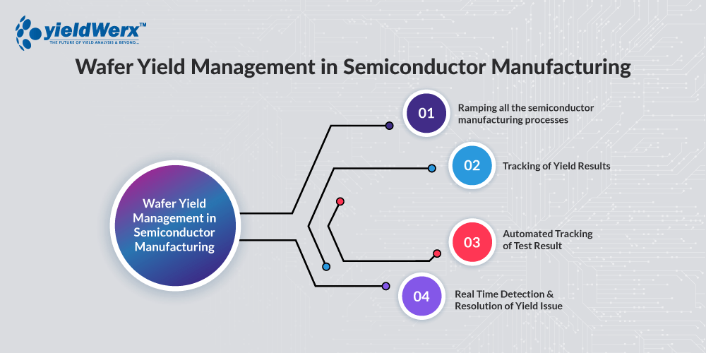
In order to increase profitability and ensure the quality of the products, it is necessary to ramp up all the semiconductor manufacturing processes and track the yield results.
Ramping all the Semiconductor Manufacturing Processes
One of the key aspects of wafer yield management is ramping all the semiconductor manufacturing processes. This includes optimizing the processes to improve the yield and increase profitability. For example, the use of new equipment, the implementation of process improvements, and the optimization of material usage are all important steps in ramping up a manufacturing process.
Tracking of Yield Results
It is essential to track the yield results to ensure that minimum acceptable thresholds are met. Yield results associated with product bins (PASS) versus scrap bins (FAIL) are monitored to ensure the products meet the required quality standards and profitability margins. This helps to identify any yield issues and take corrective actions to prevent them from occurring in the future.
Automated Tracking of Test Results
Automated tracking of test results and trends over time is also a critical aspect of wafer yield management. This helps to assess the robustness and profitability of the manufacturing processes real time. Automated identification of trends and patterns from test results in the manufacturing process that impacts yield and profitability allows for implementing real time corrective action. This prevents further yield and profit losses when the corrective actions are implemented late.
Real Time Detection and Resolution of Yield Issues
In wafer yield management, it is crucial to detect and rectify yield issues promptly using pre-established decisions and data-driven rules in real time. This approach ensures that any problems that could potentially affect the manufacturing process’s yield and profitability are swiftly dealt with. Through automation and the use of data analytics, wafer yield management can effectively enhance the manufacturing process, increase the yield, and maximize profitability.
Benchmarking with other Sites like Outsourced Semiconductor Assembly and Test (OSAT) Providers
Wafer yield management also involves comparing(benchmarking) the yield performance across internal manufacturing sites and OSAT or between OSATs This helps to optimize and manage yield results from each site at the enterprise level. It is also possible to track outsourced operations and supplier benchmarks such as foundries and OSATs. This helps to identify any issues and optimize the yield of outsourced operations.
In conclusion, wafer yield management is a critical aspect of semiconductor manufacturing. By ramping up the manufacturing processes, tracking yield results, automating the tracking of test results and trends, comparing yield across manufacturing sites, and identifying and resolving yield issues in real time, yield can be optimized, and profitability increased.