Semiconductor testing is a walk on the tightrope because of the latent defects that emerge in chips later in their life when they are part of an end-product. That’s why the discovery of a chip with a latent defect is referred to as a customer quality incident (CQI).
The stakes are even higher in industries such as automotive, aerospace and medical where reliability is crucial. Not surprisingly, therefore, statistical screening methods such as Part Average Testing (PAT) and Good Die in a Bad Neighborhood (GDBN) are now intertwined with the chip manufacturing execution system.

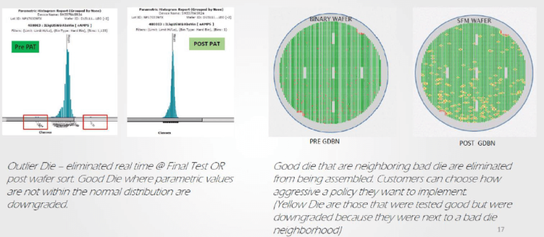
PAT, which has its roots in the automotive industry, is based on the evaluation of data from a variety of tests such as current and voltage measurements. It’s a standard industry algorithm for outlier detection that captures every die with parametric characteristic falling outside of a statistically calculated pass-fail limit.
Outlier—a chip that has passed the original manufacturing tests but differs from the lot while showing abnormal characteristics and is more likely to fail in the field—forms the basis of the PAT methodology. The outlier detection in the die-level PAT screening can be both static and dynamic.
Static PAT or SPAT technique uses a list of tests and population data from numerous batches and forms associated to lower and upper limits to screen out the dice that fall outside the specified boundary. It sets the mean (µ) and standard deviation (σ) and then defines static PAT limits as µ±6σ. The static PAT limits—called the lower specification limit (LSL) and upper specification limit (USL)—are updated every six months or eight wafer lots whichever comes first.
On the other hand, dynamic PAT or DPAT methodology calculates limits for each wafer test dynamically while computing the mean and standard deviation for each test batch individually. It’s a preferred method because the limits are calculated on the actual material being tested. A die showing values outside the dynamic PAT limits but within the LSL and USL limits is considered an outlier.
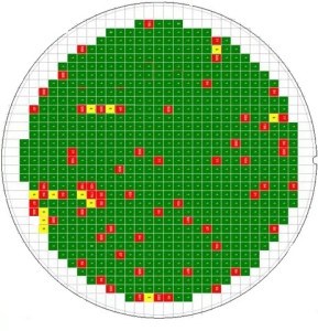
Another prominent outlier detection technique—Good Die in a Bad Neighborhood or GDBN—uses a die-level neighborhood predictive model and is based on the premise that defects tend to cluster. This screening method calculates the yield of each die and employs a weighting algorithmic recipe to remove even a good die that is surrounded by a cluster of failing dice.

Both PAT and GDBN are outlier detection schemes that use innovative algorithms to attain zero-defect quality control in chip production. However, while PAT methodology separates chips that are different from other chips, which have been normally produced, GDBN identifies a working die that is surrounded by failing dice and removes it from the lot as a precaution.
And, PAT and GDBN are two advanced manifestations of today’s semiconductor final test process, which is now combining the prowess of data mining with complex spatial algorithms to qualify test results that ensure accurate outlier detection.
Moreover, these automated screening methods are no more the exclusive domain of industries such as automotive and medical electronics. Case in point: the leading RF chipmaker Skyworks is using the PAT process to test its high-reliability wireless chips.
The PAT guidelines—originally developed by the Automotive Electronics Committee (AEC)—are hard to implement, especially at high volumes. So, the yieldWerx Enterprise lot genealogy and analysis tool provides the sophisticated workflows and tools needed to satisfy PAT test and reporting requirements.
yieldWerx’s PAT module allows test engineers to set PAT rules for parameters as well as static and dynamic limits and select data and test policy to calculate a threshold. Likewise, yieldWerx allows test engineers to set GDBN rules, carry out data selection, create GDBN filters, and change GDBN bin colors in order to map out a sophisticated neighborhood screening.
More information on static and dynamic Part Average Testing (PAT) methods is available on a yieldWerx PAT module.


