Product/Device Setup

Fabless

Advanced Product Customizations for Wafer, Reticle, and Die

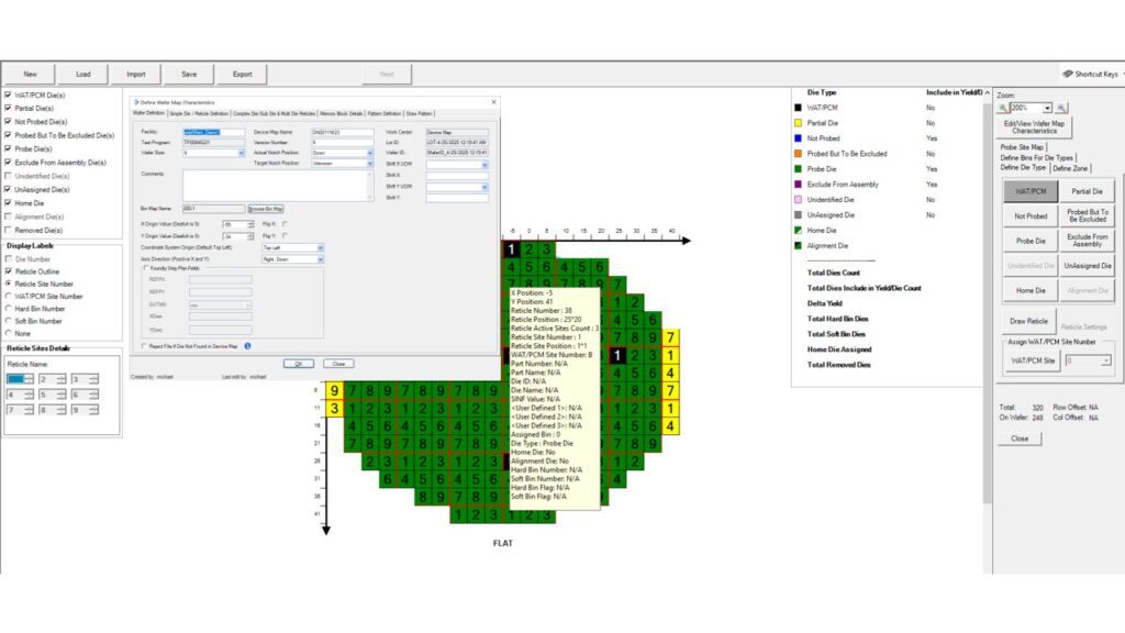
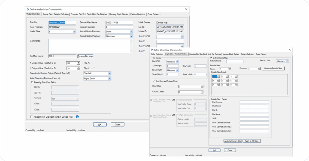
yieldWerx provides engineers with the ability to define wafer map setup, determining which dies to probe, not probe, assemble vs. unassemble, and many more. It allows engineers to mark edge dies, edge exclusion rings, probe sites, and reticle site information. yieldWerx supports multi-Project Wafers, where dies of different dimensions within a reticle shot can be defined. Advanced parameters, including Zones, can be defined and logic applied. This information can then be used to drive and control test equipment, such as optimized probing or inspection sequences/patterns (i.e., CCA – Critical Care Areas). This functionality becomes a more powerful quality improvement tool, allowing engineers to minimize the number of touchdowns made on dies. The Product/Device Setup information can be used in real-time reports and analysis, for data enrichment, or a combination of the two. The yieldWerx Product/Device Setup module also provides a unique capability for Design and Product Engineers to collaborate – GDSII to Test & Yield Management (The GDSII format supports hierarchical designs, enabling designers to create complex layouts efficiently by reusing smaller blocks.)

How Can This Module Benefit You?

Advanced and Easy-to-Use Product Customizations

Allows for unique wafer probing edge and sequence definitions for characteristics, reticle, and device 

Raw Data Enrichment 

Associates custom data to any data source and used in conjunction with real-time reports 

Real-time Equipment Control

Optimizes probing and inspection sequence/patterns i.e. CCA 
Product- Device Setup 01
Success Popup Widget
PTC-Logo

PTC

Partner

PTC is a semiconductor consulting firm based in Malaysia, providing strategic and technical consulting services to semiconductor manufacturing, assembly, test, product and ecosystem companies across Asia. yieldWerx, a leading innovator in semiconductor yield management solutions, and PTC, a premier Malaysia-based consulting firm for the semiconductor manufacturing industry, have announced a strategic collaboration to address the growing need for comprehensive data analytics across the semiconductor manufacturing lifecycle in the rapidly expanding markets of Malaysia and India.
This collaboration combines yieldWerx’s state-of-the-art analytics platform with PTC’s extensive industry knowledge and regional presence to strengthen semiconductor manufacturing capabilities across East Asia. By providing sophisticated analytics solutions tailored to regional needs, yieldWerx and PTC aim to streamline factory setup and operations, implement rigorous quality assurance protocols, and accelerate the development of sustainable semiconductor ecosystems across both countries. PTC will act as the regional consulting partner, offering advisory, deployment support, and strategic integration services to fabless clients, OSAT facilities, and manufacturing startups adopting the platform.