Quantum computing is moving out of the laboratory and into the early stages of infrastructure. Yet the path to scale will not be defined by qubit count alone. The real constraint is architectural. As quantum systems grow in complexity, performance will increasingly depend on photonic interconnects, secure communication layers, and manufacturable photonic integrated circuits capable of operating reliably at scale.
For semiconductor and photonics companies entering this space, the challenge is no longer purely scientific. It is industrial.The next generation of quantum systems will require the same rigor in yield, integration, and process control that has long defined advanced semiconductor manufacturing and by how we leverage already mature CMOS processes.
From Experimental Devices to Quantum Infrastructure
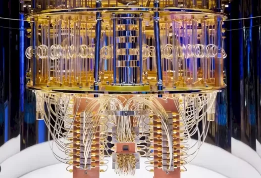
Current quantum processors remain constrained by fragility, error rates, and physical infrastructure. As systems grow larger, maintaining coherence becomes increasingly difficult. Wiring complexity increases. Thermal management becomes more demanding. Error correction overhead expands rapidly, often requiring thousands of physical qubits to support a single logical qubit.
These constraints make monolithic quantum computers impractical beyond a certain size.
The industry is therefore shifting toward a distributed model. Instead of scaling a single processor indefinitely, future quantum systems will consist of modular processors connected through photonic interconnects and secure communication channels. In this architecture, photons serve as the carriers of quantum information between nodes, enabling distributed computation and entanglement sharing across systems.
This shift mirrors the evolution of classical computing. Data centers replaced single supercomputers. Distributed cloud infrastructure replaced monolithic systems. Quantum computing is now entering a similar architectural transition.
Why Photonic Interconnects Are Essential?
Quantum systems cannot scale as single, monolithic processors. As qubit counts grow, error correction overhead, thermal management, and wiring complexity quickly become limiting factors. The practical path forward is modular architecture — multiple quantum processors connected into a larger system.
Photons are the only viable carriers for this architecture. They transmit quantum states over long distances with minimal loss and enable entanglement distribution between physically separated processors. Photonic interconnects therefore form the backbone of distributed quantum computing and networking.
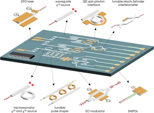
Enabling this model requires integrated platforms capable of generating entangled photons, multiplexing channels, and routing quantum states with extremely low optical loss. At this level, even small fabrication variations can reduce fidelity or entanglement rates. Precision manufacturing becomes a system-level requirement, not a process optimization.
Photonic integrated circuits (PICs) translate laboratory optics into scalable infrastructure. By leveraging the already mature CMOS processes, they can integrate waveguides, resonators, modulators, and detectors on-chip. PICs provide the optical control layer required to generate, stabilize, and distribute quantum information between modules.
Quantum hardware is transitioning towards distributed architectures and process control. Therefore, photonic semiconductor yield optimization will determine how quickly photonic technologies move from research prototypes to deployable infrastructure.
Some Applications of Quantum Photonic Interfaces
Quantum Key Distribution as the First Infrastructure Application
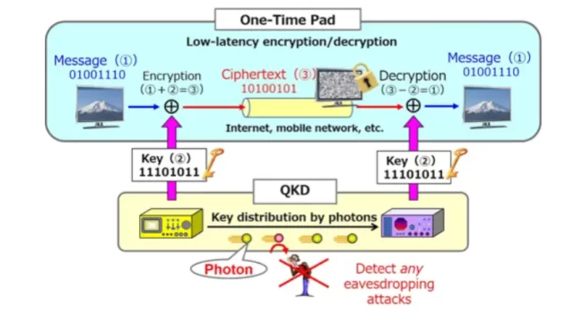
Quantum key distribution (QKD) represents one of the earliest real-world applications of quantum networking. Using quantum states of light, QKD enables two parties to generate encryption keys that are fundamentally secure against interception. Any attempt to measure or copy the quantum signal introduces detectable disturbances, ensuring communication integrity.
Unlike classical encryption, which relies on computational difficulty, QKD derives security from the laws of physics. As quantum computers advance, traditional encryption methods may eventually become vulnerable. QKD provides a path toward quantum-safe communications infrastructure.
Integrated photonic entangled photon sources are central to scalable QKD systems. These sources must generate high-quality entanglement at high rates while maintaining stability over fiber networks. Deployments are already emerging in government, defense, and financial networks where secure communication is critical.
Quantum Transduction and Cross-Platform Connectivity
Many leading quantum processors operate in physical domains incompatible with long-distance communication. Superconducting qubits, for example, function at microwave frequencies inside cryogenic environments. Optical networks, by contrast, operate at telecom wavelengths.
Quantum transduction bridges this gap. It converts quantum information between microwave and optical domains while preserving coherence and entanglement. This capability allows superconducting or trapped-ion systems to connect into larger optical networks.
As distributed quantum architectures evolve, transduction technologies will become essential for interoperability between different hardware platforms. Manufacturing these hybrid systems introduces additional integration complexity, combining microwave, photonic, and cryogenic engineering requirements.
Cryogenic Photonic Interfaces and System Integration
High-performance quantum processors operate at extremely low temperatures. Cryogenic environments minimize thermal noise and preserve qubit coherence. However, communication between these processors and external systems must still occur.
Cryogenic photonic interfaces provide this bridge. They enable photons generated inside cryogenic environments to couple efficiently into room-temperature optical networks. Designing these interfaces requires minimizing thermal load, optical loss, and mechanical instability.
As quantum systems scale into multi-module architectures, cryogenic photonics will become a critical infrastructure layer. High-density optical I/O, low-loss fiber coupling, and reliable packaging will determine how effectively quantum processors can connect and scale.
What Are the Limits to Scaling Quantum Systems Today?
Fragile Qubits & Monolithic Designs
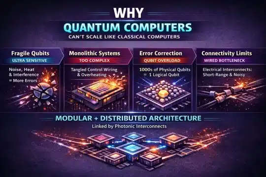
The current generation of quantum processors faces several structural limits that prevent straightforward scaling. Qubits are inherently fragile and highly sensitive to noise and environmental interference. As the number of qubits increases, so does the difficulty of maintaining coherence and controlling errors. Large monolithic quantum processors become difficult to manage due to the complexity of control wiring, thermal management, and signal integrity.
Error Correction Challenges
Error correction further complicates scaling. Reliable quantum computation requires extensive redundancy, often demanding thousands of physical qubits to create a single logical qubit capable of fault-tolerant operation. This dramatically increases system size and infrastructure requirements.
Connectivity Limits
Interconnects present another critical challenge. Quantum information must be transmitted between different parts of a system without destroying coherence. Traditional electrical interconnects generate heat and noise and cannot directly transmit quantum states over long distances. As a result, scaling quantum systems as single monolithic machines becomes impractical.
These constraints are leading to a shift in architecture. Rather than building ever-larger individual quantum processors, the industry is moving toward modular, distributed quantum systems connected through photonic technologies.
Infrastructure Opportunities in the Near and Long Term
In the near term, quantum infrastructure will expand through secure communications, sensing networks, and modular interconnect demonstrations. QKD deployments will continue to grow. Photonic interconnects will link early modular quantum processors. Packaging and integration technologies will mature rapidly.
Longer term, the industry is moving toward distributed quantum data centers and eventually global quantum networks. These systems will rely on dense photonic integration, advanced materials, cryogenic interfaces, and robust manufacturing processes.
Enabling Scalable Quantum Photonics Through Yield and Process Control
The shift from experimental photonic devices to deployable quantum infrastructure introduces a fundamental requirement: manufacturability at scale. Photonic integrated circuits for quantum systems must meet stringent performance requirements while maintaining consistent yield across production runs.
In this case, photonic yield management platforms help by:
- Improve qubit uniformity
- Increase usable qubits per wafer
- Track process-induced decoherence risks
- Optimize phase stability and photonic waveguide loss
- Ensure manufacturing consistency at scale
Real Examples of Process Optimization Improving Quantum Performance
PsiQuantum
Quantum computing performance can be significantly improved through conventional semiconductor process optimization, design-for-manufacturing, and large-scale photonic integration. The PsiQuantum team did it without relying completely on quantum physics.
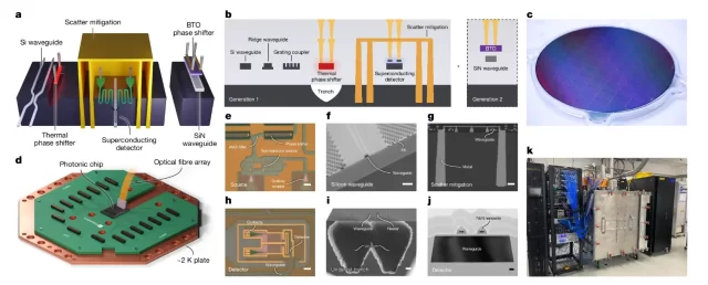
This Palo Alto–based startup unveiled new details about its photonic quantum chipset, “Omega,” in a scientific paper published in Nature. Designed specifically for utility-scale quantum computing, Omega represents a major step toward scalable quantum hardware.
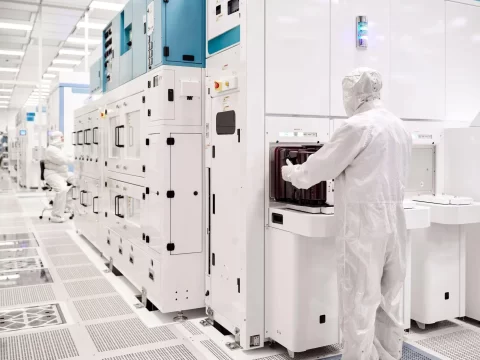
The paper describes a chipset designed and manufactured on full-size silicon wafers at GlobalFoundries’ silicon photonics fabrication facility. The platform integrates several critical components, including high-performance single-photon sources, superconducting single-photon detectors, and a next-generation optical switch built using barium titanate, all engineered to support large-scale photonic quantum systems.
By using a 300-mm silicon photonics foundry flow, they achieved:
- Higher uniformity → more usable qubits
- Repeatability → higher entanglement fidelity
- Integration of critical components (such as photon sources, waveguides, detectors, filters, and phase shifters) onto a single chip → stability
They also engineered fabrication-tolerant photon sources and introduced lower-loss materials like silicon nitride to minimize variability and reduce the need for post-fabrication tuning.
IBM
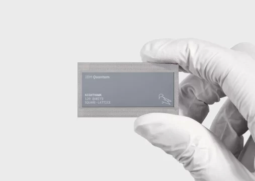
As IBM scaled from Falcon and Hummingbird processors to the 127-qubit Eagle and the new 120-qubit Nighthawk chips, it refined packaging and manufacturing processes such as multi-layer wiring, through-silicon vias, and advanced signal routing to reduce classical crosstalk and improve qubit isolation.
These improvements enhance coherence times, gate fidelity, and readout accuracy across larger qubit arrays. Eagle demonstrated coherence times exceeding 400 microseconds while nearly doubling processor scale, and Nighthawk’s square-lattice topology increases couplers from 176 to 218, enabling circuits that are about 30% more complex with fewer SWAP operations.
IBM’s Heron processors further show the impact of iterative optimization, achieving up to 330,000 circuit layer operations per second (CLOPS) and delivering two-qubit error rates below 0.1% on dozens of couplings, enabling utility-scale experiments to run over 100× faster than in 2023.
These performance gains are driven by continuous process and design refinement across the entire quantum stack. IBM’s transition to advanced 300 mm wafer fabrication has cut wafer processing time in half and accelerated R&D cycles, allowing the company to build chips up to 10× more complex while rapidly integrating lessons from each hardware revision.
Together, these tightly integrated process optimizations across hardware, fabrication, and software demonstrate how disciplined engineering and manufacturing improvements are essential to scaling qubit counts, reducing errors, and achieving reliable, high-performance quantum computing on the path toward fault-tolerant systems.
How yieldWerx Enables Manufacturable Quantum Photonics at Scale
yieldWerx provides photonic yield analytics, process visibility, and yield management capabilities required to support this transition. By enabling deeper insight into photonic fabrication processes and variation sources, yieldWerx helps photonics manufacturers accelerate development cycles, improve device consistency, and scale production of advanced PICs.
For organizations building the optical backbone of quantum computing and networking, yield management is no longer optional. It is foundational.
Quantum computing will scale through photonic interconnects, secure communication layers, and modular architectures. The companies that can manufacture these systems reliably and at scale will define the next phase of the quantum industry.
Connect with yieldWerx to explore yield-driven quantum photonics at scale.
FAQs
What is Quantum Computing?
Quantum computing uses quantum mechanical effects to process information in ways that classical computers cannot. Instead of binary bits, it uses quantum bits (qubits) to solve certain problems in optimization, materials science, cryptography, and simulation far more efficiently than traditional systems.
What are the Benefits of Quantum Computing?
Quantum computing can solve certain complex problems much faster than classical computers. It is expected to improve areas such as drug discovery, materials design, optimization, artificial intelligence, and secure communications by processing large and complex datasets more efficiently.
Quantum computers are not faster for everyday tasks, but for specific problems they can be dramatically quicker. Some calculations that would take classical supercomputers years could eventually be solved by advanced quantum systems in minutes or hours.
What are Qubit Types?
Qubits can be implemented using several physical technologies. The main types include superconducting qubits, trapped ions, neutral atoms, photonic qubits, and spin-based qubits. Each platform differs in coherence time, scalability, operating temperature, and integration complexity.
What is Quantum Entanglement?
Quantum entanglement is a phenomenon where two or more particles become correlated so that the state of one instantly determines the state of another, regardless of distance. It is a fundamental resource for quantum computing, secure communication, and quantum networking.
What are Quantum Networks?
Quantum networks connect quantum devices using entangled photons transmitted through optical fiber or free space. These networks enable secure communication, distributed quantum computing, and the future development of a quantum internet linking processors and sensors across large distances.
What is Quantum Photonics?
Quantum photonics is the use of light (photons) to generate, manipulate, and transmit quantum information. It includes technologies such as photonic integrated circuits, entangled photon sources, and optical interconnects that form the communication and networking layer of scalable quantum systems.
What are Cryogenic Temperatures?
Cryogenic temperatures refer to extremely low temperatures, typically near absolute zero (−273°C), used to operate many quantum processors such as superconducting qubits. These environments reduce thermal noise and preserve quantum coherence, allowing qubits to function reliably.
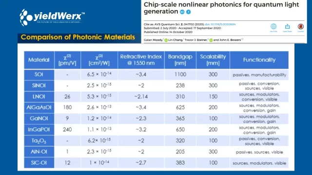
What are The Top Photonic Materials Used For Quantum Computing?
Key photonic materials used in quantum computing include silicon and silicon nitride for scalable, low-loss photonic integrated circuits, lithium niobate for high-speed modulation and photon generation, and indium phosphide and GaAs for efficient single-photon sources and detectors. Emerging materials like barium titanate support advanced optical switching.
Many leading quantum photonic platforms are built on insulator substrates.
The most common examples are:
- Silicon-on-Insulator (SOI)
- Silicon Nitride-on-Insulator (SiN-on-insulator)
- Lithium Niobate-on-Insulator (LNOI)
The insulating layer (usually silicon dioxide) confines light strongly in the waveguide, reduces optical loss, improves phase stability, and enables dense integration — all critical for scalable, high-fidelity quantum photonic circuits.
List of References: