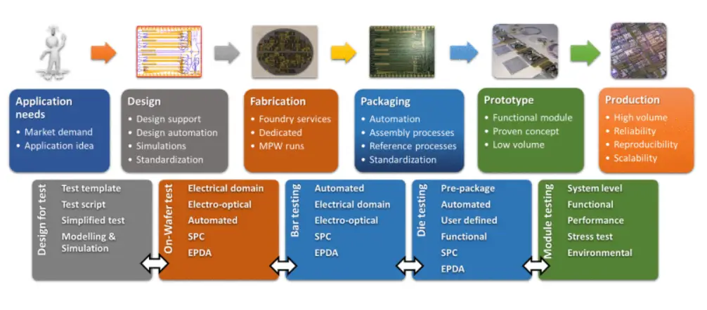
Semiconductor industries typically evolve in phases. The first phase is driven by device innovation. The second is driven by ecosystem development and process stabilization. Eventually, however, large-scale commercialization depends on manufacturing standardization, testing scalability, and connected data infrastructure. Silicon photonics is now approaching that third phase.
Silicon photonics is entering a new phase of industrial growth. What was once viewed primarily as a niche technology for telecommunications is now becoming a foundational technology for AI infrastructure, co-packaged optics (CPO), quantum computing, lidar, biosensing, and next-generation datacenter interconnects.
As the industry scales, however, a major problem is becoming increasingly visible. Silicon photonics has achieved partial standardization in design and simulation, but the manufacturing side of the ecosystem remains deeply fragmented. The closer the industry gets to real-world production and testing, the more disconnected the workflows become.
This fragmentation is no longer simply an engineering inconvenience. It is becoming a major constraint on silicon photonics scalability, yield learning, test efficiency, root-cause analysis, and manufacturing cost reduction.
The challenge is the inability to consistently connect manufacturing data across different tools, process stages, testing systems, and engineering domains.
What Is The Current State of Standardization in Silicon Photonics?
Some parts of the ecosystem are relatively mature and standardized, while others remain highly customized and fragmented. The most standardized parts of silicon photonics are largely inherited from the semiconductor industry itself.
At the layout level, most photonic designs still rely on GDSII and OASIS file formats. These formats are used to define the physical geometries that are ultimately transferred to masks and fabricated in foundries. Because they originated in the CMOS world, they already possess decades of industrial maturity and interoperability.
Similarly, simulation and modeling workflows have inherited some level of standardization from RF and semiconductor engineering. Touchstone files and S-parameter representations are widely used for frequency-domain modeling and optical characterization. These formats allow designers to exchange behavioral models and simulation results across different environments.
Process Design Kits (PDKs) have also become relatively common in silicon photonics. Many foundries now provide libraries containing waveguides, couplers, splitters, modulators, and design rules that designers can reuse. This creates a degree of portability and repeatability, especially on silicon-on-insulator (SOI) platforms where 220nm silicon thickness has become relatively common.
However, even here the standardization is only partial. Each foundry still maintains its own:
- doping profiles
- etch depths
- fabrication tolerances
- thermal tuning behavior
- component libraries
- process recipes
As a result, designs often require re-optimization when moving between different fabs.
In the last few years, GdsFactory has gained traction as an open-source framework for photonic layout and simulation workflows through its Gplugins ecosystem, While it has not yet emerged as a universal standard, it reflects growing industry interest in more interoperable and scalable photonic design environments. Despite some fabs still refusing layouts made by GdsFactory, the platform has the potential of getting towards more standardized workflows.
Standardization Efforts Are Global, But the Ecosystem Remains Fragmented
Silicon photonics standardization is not limited to a specific region. Efforts are taking place globally.
Organizations such as theIEEE Photonics Standards Committee are actively working on terminology, testing methodologies, and interoperability frameworks. Europe has invested heavily in initiatives such as openEPDA and photonic design automation interoperability. Meanwhile, the United States and Asia continue pushing commercial deployment of co-packaged optics and high-volume photonic manufacturing.
Yet despite this global activity, the ecosystem still lacks convergence.
Different foundries, packaging houses, hyperscalers, and testing labs often operate with completely different workflows and internal standards. In many cases, companies intentionally keep portions of their manufacturing and testing methodologies proprietary because they represent competitive advantages.
The result is an industry that resembles a loosely connected network of specialized ecosystems rather than a unified manufacturing infrastructure.
The Real Problem Starts at Manufacturing
The most important insight emerging across the industry is that standardization begins to break down as soon as the device enters manufacturing and testing.
At the design stage, workflows are relatively structured. Designers work with controlled simulation environments, standardized layout representations, and reusable component libraries.
Once manufacturing begins, however, the environment becomes dramatically more complex.
A modern silicon photonics manufacturing flow generates enormous amounts of heterogeneous data. This includes:
- optical spectral measurements
- thermal characterization
- packaging and alignment data
- image-based defect inspection
- X-ray metrology
- process chamber information
- fiber alignment signatures
- wavelength sweeps
- drift analysis over time
Each of these datasets may come from different vendors, different tools, different teams, and different process stages.
More importantly, they often use completely different data structures.
One dataset may exist at wafer level, another at die level, another at optical port level, and another at wavelength level. Some systems preserve coordinate information while others do not. Some tools output structured databases while others produce CSV or JSON files. Some optical systems store spectral curves while others reduce results into simplified pass/fail metrics.
The problem, therefore, is that the data rarely connects cleanly across the manufacturing chain.
Why Has Cross-Domain Correlation Become So Difficult?
This fragmentation creates major problems for silicon photonics yield analysis, root-cause investigation, and manufacturing scalability.
Consider a relatively simple manufacturing question:
Why did a die that passed wafer testing later fail as a packaged optical module?
Answering this question may require engineers to correlate data types mentioned above. But in many organizations, these datasets exist in isolated systems that do not naturally communicate with one another.
Electrical data may be stored using mature semiconductor test infrastructures. Optical data may exist in custom lab-generated formats. Alignment information may not even be preserved after packaging. Inspection images may have no standardized linkage back to wafer coordinates or optical ports.
This creates what many companies now describe as a broken digital thread.
The genealogy of the device becomes fragmented as it moves from:
Design → Fabrication → Wafer test → Packaging → Final test → Deployment
Once that continuity breaks, correlation becomes slow, manual, and heavily dependent on tribal engineering knowledge. This challenge becomes even more severe in heterogeneous integration environments where photonic dies, electronic ICs, chiplets, advanced substrates, and optical interfaces must all be correlated within the same manufacturing genealogy.
Testing Has Become the Industry’s Biggest Bottleneck
Testing is increasingly emerging as the area where the lack of standardization is most painful.
Unlike conventional semiconductor testing, silicon photonics testing involves both electrical and optical domains simultaneously. Optical alignment itself introduces entirely new layers of complexity.
A photonic device may contain multiple optical lanes, each requiring extremely precise alignment between fibers and waveguides. Even micron-level shifts can significantly impact coupling efficiency and final performance.
As optical lane counts increase, testing time and complexity scale rapidly.
The industry still lacks a universally accepted methodology for:
- wafer-level optical testing
- alignment procedures
- optical port characterization
- multi-fiber testing
- thermal compensation during optical measurements
Many companies therefore, build highly customized testing environments internally. These systems often combine:
- custom probe stations
- proprietary alignment methods
- internally developed scripts
- vendor-specific optical equipment
- manually integrated workflows
While these environments may work for specific products, they are difficult to scale across the broader industry.
This is one reason silicon photonics testing costs remain dramatically higher than traditional semiconductor testing.
Alignment Data Is One of the Most Overlooked Problems
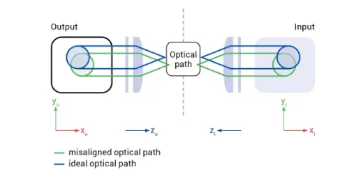
One particularly important issue is alignment metadata.
Optical alignment data may include:
- fiber positions
- Z-heights
- angular offsets
- coupling efficiency
- thermal alignment behavior
Yet this information is often poorly preserved or disconnected from the device genealogy. As a result, engineers may identify a failed optical module without being able to determine the root cause.
This inability to maintain traceable correlations across domains is becoming one of the largest manufacturing obstacles in the industry.
Why Silicon Photonics Standardization Remains an Economic Challenge?
One of the biggest barriers to silicon photonics standardization is not technology, but economics.
Semiconductor testing is typically about 10% of component costs, according to some estimates, silicon photonics testing can be anywhere from 60% to 90% of product costs.
While major companies already have the capability to build highly precise photonic manufacturing and test systems, the industry remains too fragmented for many solutions to be easily reused across customers.
Different companies often rely on unique packaging methods, optical interfaces, alignment schemes, and test flows, forcing vendors to heavily customize systems for nearly every deployment.
This lack of standardization increases non-recurring engineering (NRE) costs and slows time-to-market.
To address this, organizations are exploring modular approaches built around open APIs, standardized layout templates, common I/O definitions, and interoperable data exchange formats. The goal is not complete uniformity, but enough standardization to make photonics manufacturing and testing more scalable while still allowing room for customization and innovation.
How yieldWerx Is Addressing the Standardization Gap in Silicon Photonics?
As silicon photonics and co-packaged optics move toward volume manufacturing, yieldWerx has built its platform around the idea of a unified digital thread.
Rather than forcing companies to replace their existing infrastructure, yieldWerx supports both greenfield and brownfield implementations, allowing customers to either build new workflows from scratch or integrate existing databases, analytics pipelines, and internal manufacturing systems into a unified framework.
Moreover, yieldWerx performs correlation analysis across the full manufacturing stack, including fab data, PCM data, defect inspection data, wafer sort data, and final test data, regardless of whether the source is chamber data, recipe data, slot data, parametric measurements, or yield data.
In addition, the company positions its platform around bi-directional traceability between design and manufacturing, allowing engineers to correlate design changes against downstream yield behavior and manufacturing performance or vice versa. This enables teams to analyze how yield shifted before and after a design or process modification and trace potential root causes.
Capabilities such as the yieldWerx lot disposition module are designed to automate analysis across optical and electrical datasets to identify yield risks, spectral drift behavior, alignment signatures, and reliability anomalies.
Combined with AI-assisted analytics, the broader goal is to reduce the highly manual debugging and cross-domain correlation workflows that still dominate much of the silicon photonics manufacturing ecosystem today.
Conclusion
Silicon photonics has already achieved meaningful progress in layout formats, simulation frameworks, and certain aspects of design reuse. But the manufacturing side of the ecosystem remains fragmented, particularly when it comes to testing, alignment, genealogy, and cross-domain data correlation.
The industry’s biggest unsolved problem is no longer simply photonic device performance.
It is manufacturing data consistency.
As silicon photonics moves toward large-scale deployment in AI datacenters, co-packaged optics, optical interconnects, and heterogeneous integration systems, the ability to connect optical, electrical, thermal, alignment, packaging, and inspection data into a unified manufacturing infrastructure may become the defining challenge of the next decade.
Until that gap is solved, silicon photonics will remain an industry with increasingly advanced devices operating on highly fragmented manufacturing workflows.
Is Fragmented Manufacturing Data Slowing Your Silicon Photonics Ramp?
yieldWerx helps photonics companies unify optical, electrical, process, and test data into a connected digital thread designed for faster yield learning, root-cause analysis, and scalable manufacturing. Book a Demo Today.
References:
SPEA: The Evolving Landscape of Silicon Photonics Testing
Standards: The Next Step For Silicon Photonics
Open Standards for Automation of Testing of Photonic Integrated Circuits
FAQs
What is BOM?
BOM stands for Bill of Materials. When we say testing can be “90% of the BOM” in silicon photonics, we mean that testing accounts for an extremely large portion of the product’s total manufacturing cost — sometimes approaching the cost of all other components combined.
What is alignment in silicon photonics?
In silicon photonics, alignment refers to the precise positioning of optical components such as fibers, waveguides, and photonic chips so light can efficiently travel between them. Even micron-level misalignment can cause signal loss, lower coupling efficiency, or device failure, making alignment one of the biggest challenges in photonics manufacturing and testing.
Why is optical alignment considered one of the biggest manufacturing challenges?
Optical alignment requires micron-level precision between fibers, waveguides, and optical ports. Small positional shifts can significantly affect coupling efficiency and module performance. Alignment data is also often poorly preserved across workflows, making failures difficult to trace later.
Why are silicon photonics testing costs so high?
Unlike conventional semiconductor testing, silicon photonics testing combines optical and electrical validation while also requiring precise fiber alignment and thermal compensation. Many companies still rely on custom-built testing environments, which increases complexity, engineering effort, and cost.
What are greenfield and brownfield implementations in photonics manufacturing?
Greenfield implementations involve building new manufacturing data infrastructures from scratch, while brownfield implementations integrate existing tools, databases, analytics pipelines, and manufacturing systems into a more unified workflow without replacing everything.


