KLARF File Format: Enhancing Semiconductor Yield Analysis with yieldWerx
Understanding the KLARF File Format
In the semiconductor industry, a KLARF file (KLA-Tencor Advanced Results File) is a specialised file format used to store data collected from semiconductor wafer inspection and metrology systems.
KLARF files contain critical defect-related information, including:
- Defect Data: Location, type, and size of defects detected on the wafer.
- Inspection Conditions: The settings and parameters used during the inspection process.
- Metrology Data: Measurement details of various semiconductor parameters.
These files enable test engineers to analyse defects at different semiconductor manufacturing stages, ensuring yield optimization and high product quality. Fabs and IDMs are the primary users of KLARF files.
KLARF files are typically processed with specialized software tools that assist in reticle/mask defect inspection, analysis, and classification. It incorporates elements of a wafer map while also providing detailed defect location data within each device—an aspect not supported by other map file formats. You can easily use it to transfer coordinates of defect maps across different inspection stages. Additionally, the KLARF file includes references to bitmap images of defects, making it a hybrid between a database and a visual defect analysis tool.
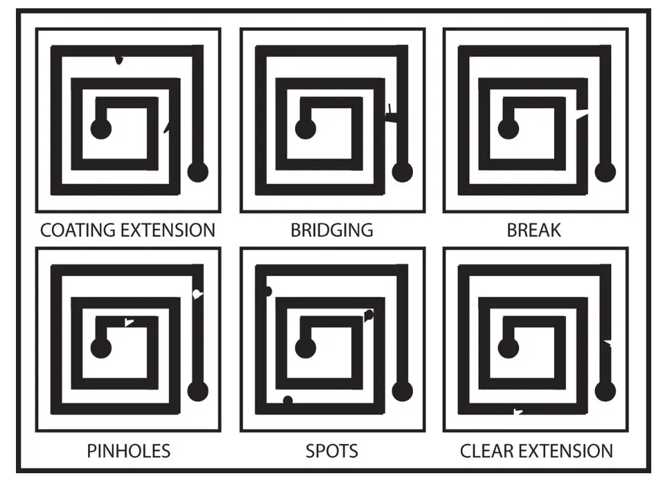
A defect-free reticle, also known as a photomask or mask, is essential for ensuring high semiconductor device yields, as any defects or pattern misplacements on the reticle can be replicated across multiple dies on production wafers.
In this blog post, we’ll explore some of the challenges yield engineers face in handling the Klarf file format and how yieldWerx provides an effective solution.
Challenges Before Implementing yieldWerx
Before the adoption of advanced yield analysis software like yieldWerx, semiconductor manufacturers encountered several significant challenges:
1. Manual Data Handling
Semiconductor wafer inspection and metrology tools generate vast amounts of data. Manually managing and analyzing this data is overwhelming and inefficient. This approach was tedious, prone to human error, and lacked scalability.
2. Slow Decision-Making
The absence of automation and integrated analysis tools led to delays in identifying defect root causes. This, in turn, slowed down corrective actions, impacting production efficiency.
3. Inconsistent Defect Classification
Defect classification varied between engineers due to manual interpretation, leading to inconsistencies in data analysis and subsequent process improvements.
4. Limited Cross-Department Communication
Data was often siloed within different teams, such as process engineering and quality control. This lack of integration caused inefficiencies and misaligned defect resolution strategies.
How yieldWerx Enhances Wafer Mapping With KLARF Data Format
Here’s how yieldWerx helps with KLARF file format data analysis:
1. Automated KLARF Data Ingestion & Integration
yieldWerx automatically ingests KLARF files, extracting wafer map data, defect locations, inspection parameters, and metrology results. Our powerful module eliminates the need for manual file uploading and ensures consistent, structured data processing from various inspection tools, not just those made by KLA.
This module provides reports like Defect Wafer Maps, Zonal Maps, Trend, and Histogram, which aid in the analysis.
2. Centralized Data Management for Efficient Analysis
yieldWerx consolidates KLARF data from multiple wafers, lots, and tools into a single database, enabling engineers to analyze defect trends and process variations over time. This centralized repository improves traceability and helps in root cause analysis. Our Defect Data Management Module is at the heart of the solution.
3. Advanced Visualization & Wafer Mapping
The system displays wafer maps with defect overlays, allowing engineers to efficiently identify defect clusters and analyze spatial distribution. Interactive heatmaps and defect density charts further aid in detecting problem areas and process anomalies.
Additionally, engineers can apply filters and layers to focus on specific defect types, size ranges, or process conditions, enabling more targeted troubleshooting.
4. Intelligent Defect Classification & Pattern Recognition
The system identifies recurring defect patterns, enabling engineers to correlate defects with specific process steps, equipment, or materials. It also supports rule-based and statistical classification methods, ensuring accurate and repeatable defect analysis for improved process control and yield optimization.
5. Automated Reporting & Trend Analysis
yieldWerx automates defect reports based on KLARF file data, reducing manual effort and improving accuracy. Yield engineers can track defect density trends, process variability, and yield impact over multiple production runs.
6. Cross-Department Collaboration & Decision Support
Provides real-time dashboards that integrate defect data, enabling quality control, and process engineering teams to work together effectively. Custom alerts and notifications help teams take proactive corrective actions when defect thresholds are exceeded.
7. Faster Time-to-Decision & Improved Yield
By automating KLARF data ingestion, visualization, classification, and reporting, yieldWerx enables semiconductor manufacturers to:
✔ Identify defects earlier
✔ Detect process drift quickly
✔ Reduce scrap and rework costs
✔ Optimize yield and production efficiency
Value Addition with yieldWerx
By implementing yieldWerx, semiconductor manufacturers experience significant improvements across multiple areas:
1. Improved Yield
Early and accurate defect identification allows for faster corrective actions, leading to better yield rates and reduced production costs.
2. Faster Decision-Making
Automated analysis and reporting accelerate decision-making, reducing downtime and enabling timely process optimizations.
3. Enhanced Accuracy and Consistency
Automated defect classification eliminates human subjectivity, ensuring uniform and reliable defect analysis.
4. Better Traceability
With centralized defect data, engineers can track recurring issues over time, helping to optimize manufacturing processes and prevent yield losses. Our Lot Genealogy Module manages this flawlessly.
By leveraging yieldWerx, semiconductor manufacturers gain a competitive edge in an industry that demands ever-higher precision and efficiency. The ability to automate and optimize defect analysis with KLARF file processing ensures higher yield rates, cost efficiency, and enhanced product reliability.
If you are faced with a format you can’t convert or don’t recognize, please send us a sample or two. We will be glad to see if it matches an existing format we support.
Contact us today and see how yieldWerx can transform your defect data management strategy.