

What happens to the semiconductor industry when some of its biggest customers start defining their own processors? While companies like Google, Amazon, Microsoft, and Meta still depend on commercial GPUs, they are increasingly adopting custom AI chips around their workloads.
For semiconductor companies, that creates a different kind of customer: one that arrives with architectural requirements and looks to the industry’s expertise to make them real.
Meta’s work with Broadcom gives this shift a practical form. Meta knows which operations its AI services perform and what its future infrastructure needs to support. Broadcom contributes expertise in chip design, networking, and packaging.
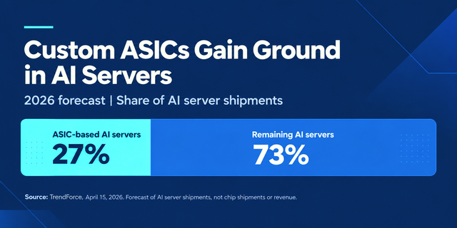
This and similar arrangements are opening custom AI chip development to a wider network of specialist firms. Although GPU-based systems still represent the larger share, a growing part of AI computing is being built around customer-directed silicon. TrendForce forecasts that ASIC-based systems will account for roughly 27% of AI server shipments in 2026.
This transition gives processor developers greater control over silicon. It also creates a compelling performance and cost advantage. For semiconductor businesses that help build them, it creates new work as well as new dependencies.
For instance, a hyperscaler may control the features that differentiate a chip, while companies like Broadcom, Marvell, and TSMC contribute the expertise needed to build it.
The shift from design to a qualified device explains the industry shift. It begins with the economics of choosing an ASIC over a GPU, passes through a distributed development model and advanced packaging, and concludes with the production data required to maintain yield at scale.
When Does a Custom AI Chip Make More Sense Than Using GPUs
A commercial GPU has one advantage that matters when AI models change quickly: a GPU bought for today’s AI models can stay useful long after those models evolve. A company might train one generation of models on its existing hardware, experiment with an entirely different architecture six months later, and eventually shift some of that computing capacity toward inference.
NVIDIA and AMD have spent years building the programming tools and libraries that make this transition possible, and customers have good reasons to value that flexibility. Nobody can predict with much confidence what AI workloads will look like several years from now.
But consider a hyperscaler that already knows where a large share of its computing budget goes. Engineers can study repeated operations, calculate the numerical precision they need, and identify where memory transfers consume power.
Custom AI chips allow engineers to design hardware tailored to specific workloads. An application-specific integrated circuit (AI ASIC) can be optimized for targeted operations, enabling precise configuration of processing units, memory hierarchies, numerical precision, and data movement.
Significant cost savings are possible at hyperscaler scale. For example, Google’s first Tensor Processing Unit (TPU), deployed in 2015 for neural-network inference, focused silicon resources on matrix multiplication. In a 2017 study, Google reported 15 to 30 times the performance and 30 to 80 times the performance per watt compared to contemporary CPU and GPU systems on production inference workloads.
These numbers describe a historical comparison, including NVIDIA’s K80, rather than a performance advantage over current GPUs. They show what was possible when architects already understood the computation their processor would spend its life performing.
It takes more than an efficient chip design just to save money. Since custom silicon involves substantial development costs, the hardware has to remain busy for a sufficient length of time in order to recoup that investment. The financial benefit can vanish even if the chip performs precisely as expected, simply because the workload changes greatly or demand is less than expected.
ASIC vs GPU: The Decision in Practice
| Consideration | Commercial GPU | Custom AI ASIC |
| Workload | Broad, changeable mix | Large, reasonably predictable demand |
| Hardware | Programmable platform with established software | Compute, memory, and interconnect tailored to selected applications |
| Investment | Purchase and deploy an existing product | Fund design, verification, software, tape-out, and qualification |
| Principal risk | Paying for flexibility or capacity that goes unused | Failing to recover development cost if demand or models change |
| Potential advantage | Faster adoption and reuse | Lower cost per useful computation at sufficient scale |
The comparison captures technical trade-offs, but financial decision takes place over years. A hyperscaler should compare full cost of buying and operating GPUs with the nonrecurring engineering expense of building an ASIC, the cost of its software stack, power and networking requirements, utilization, and the number of qualified processors it can actually deploy.
To sum up, purchasing GPUs eliminates the risk of creating an architecture that becomes obsolete before it has paid for itself, whereas if you own the design it will pay off provided that the workload stays stable and is large enough.
A recent analysis by McKinsey suggested that inference ASICs could cut the cost per token by 70-80% for their intended workloads under certain assumptions. These potential savings could shrink with lower deployment volumes, shifts in model architecture, or poor manufacturing yields.
It therefore explains why the hyperscalers are incorporating custom silicon into their range while at the same time purchasing commercial GPUs.
A company that accepts those costs is making a second decision at the same time. It wants control over the features that distinguish its processor, but it does not necessarily want to own every design tool, interface block, or manufacturing operation required to build one.
That is where the broader semiconductor market is beginning to change.
How is Semiconductor Development Model Changing
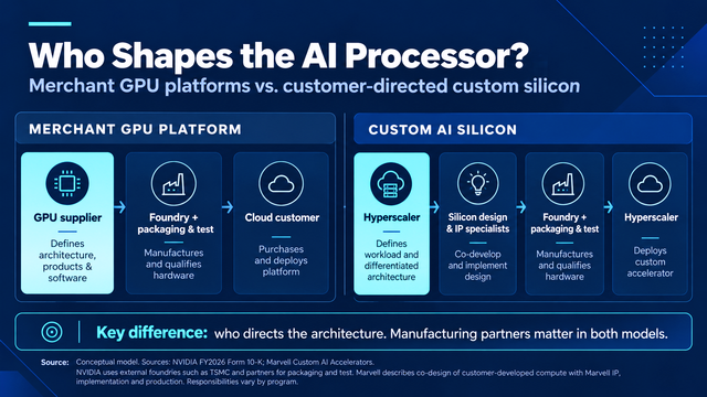
The familiar merchant GPU model puts product architecture and the software roadmap in the hands of a supplier such as NVIDIA, and the customers buy the resulting platform. NVIDIA already uses external foundries, assembly specialists, and test partners, so the new development should not be confused with a move away from in-house manufacturing. What is changing is who directs the differentiated architecture, i.e., the customers.
In a customer-directed program, a hyperscaler may design the compute engine, set performance targets, and define software requirements, then work with specialists for IP, verification, physical implementation, and other parts of the chip.
Marvell’s custom AI accelerator is one example of this approach, with customers able to bring their own compute designs while drawing on Marvell’s experience in memory systems, interconnects, packaging, and implementation. The arrangement lets a hyperscaler focus its engineering resources on the architecture that makes its custom processor worth building, leaving much of the supporting work to engineers who specialize in it.
Broadcom’s work with Meta shows another form of collaboration. Foundries such as TSMC fabricate the dies, while packaging and test providers contribute the remaining steps needed to deliver qualified hardware. IP ownership and the work allocated to each party vary by program.
For companies offering semiconductor, IP verification, physical implementation, die-to-die connectivity, or outsourced assembly and test, this creates a more substantial route into AI computing.
A hyperscaler no longer has to replicate each specialised engineering function in order to bring its own processor online. It still requires a large amount of capital, design expertise, and a sufficiently large deployment if the project is to be worthwhile. What it can do instead is gather the necessary skills from different companies rather than keeping them all under one roof.
The transition leads to a change in competition. Commercial GPU suppliers compete on processor performance, pricing, availability, and their software ecosystems, while Custom silicon specialists work to secure long-term development programs, reusable IP placements, and implementation contracts.
Meanwhile, foundries and packaging providers compete for capacity-intensive advanced products. Hyperscalers purchasing merchant GPUs may also commission custom accelerators, giving different suppliers a place in their infrastructure strategy.
In one report, TrendForce forecasts 24.8% growth in foundry revenue for 2026, with AI processors helping drive demand. Its later server-market analysis described component lead times growing as suppliers prioritized AI-related orders.
However, these opportunities have their own drawbacks. Although a new custom accelerator can bring in business for a design company, it at the same time places pressure on the capacity of the foundry, packaging, and testing that other customers require. Similarly, changes in a major hyperscaler’s schedule can affect those suppliers.
The work can be shared, but AI chip design to produce a single working system. The compute logic, memory, and connectivity cannot be optimised independently simply because different specialists are responsible for them. That physical limitation is what leads to the use of chiplets and advanced packaging.
Also Read: Why Semiconductor Startups Need Yield Analytics Earlier Than They Think
Why Chiplets and Advanced Packaging Matter for AI Accelerators
An AI accelerator can have enormous computing capacity and still spend much of its time waiting for data. Moving that data between devices also consumes power, sometimes enough to undermine the efficiency gains that the chip was designed to deliver. Memory interfaces, interconnects, and advanced packaging therefore deserve as much attention as the compute engine itself.
That is where chiplets come into play. A large AI accelerator doesn’t have to be built on a single die. With chiplets, designers can separate compute, input/output (I/O), and supporting circuitry using different process technologies for each. But the actual difficulty is getting those dies to communicate efficiently.
TSMC’s CoWoS technology addresses this problem by placing high-performance logic dies and high-bandwidth memory (HBM) in one package, linked through dense interposer connections. TSMC says this lets data move within the package instead of traveling over longer board-level paths.
Both commercial GPUs and custom AI chips use these packaging techniques. The distinction lies in the architectural choices they enable, not in exclusive ownership of the technology.
Custom programs can add pressure of their own, such as newer designs, lower early volumes, and more suppliers contributing to a single package, all of which make the learning curve harder to shorten.
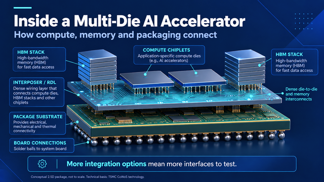
The possible designs are becoming much larger. Marvell announced its modular packaging platform, which could accommodate multi-die accelerator designs with 2.8 times the silicon area of a conventional single-die implementation.
This flexibility matters when customers want to combine differentiated compute, memory, and connectivity in a specific configuration. But when a die boundary makes an architecture practical, it also creates a physical interface with demanding electrical and reliability requirements.
Yes, the chiplets can improve fabrication economics by replacing some large dies with smaller ones which are easier to manufacture and test. However, this approach transfers part of the engineering workload to the assembly process; for instance, the bonds may become misaligned, the interfaces might fail, heat can have an effect on adjacent components, and if a problem is found after integration it could put several valuable dies at risk.
The financial case for a multi-die accelerator therefore depends on how many complete, qualified packages the manufacturing process can deliver. And that is not all; multiple manufacturing challenges can disrupt AI chip yield. That is where yield engineering becomes central to the custom chip business case.
Also Read: Chiplets: The Building Blocks of Sustainability
The Manufacturing Challenges Behind AI Chip Yield
Consider what happens as a new accelerator moves toward volume production. A foundry has fabricated its logic dies. Wafer sort identifies parts that meet their initial electrical limits. Known Good Die (KGD) screening helps decide which are worth packaging with expensive memory and other components. The assembled device must then pass tests that could not be performed on its constituent dies alone. Each step adds cost, and the later a defect escapes, the more of that investment is at risk.
The engineering difficulties keep shifting along the route:
- Fabrication and wafer variation. Differences in process conditions can push frequency, leakage, or power outside specification, even where a die remains functional.
- Screening and die selection. More tests can catch marginal parts before assembly, but they also consume time and may reject material that would otherwise meet final requirements.
- Package integration. Bonding, contamination, thermal interactions, and interconnect faults can cause a multi-die package to fail even when individual dies appear functional.
- Final qualification. Engineers must validate the complete device, including electrical paths and system behaviors that could not be tested at wafer sort.
The product team has to manage these stages across different suppliers.
- A die can satisfy wafer-sort criteria at one location while the final package falls short of the customer’s requirements at another.
- Changing a screening threshold may reject more material upstream, but it may also avoid greater losses after assembly.
Finding the right balance requires more than a passing report from each supplier; it requires evidence about what happens to devices after they leave one process and enter the next.
This is where the economics that justified the chip at the outset return in a different form: a highly efficient architecture is worth less if too few good devices survive production.
The next question is how a product team learns quickly enough to improve that result. A final test can reveal that a device failed, but it may not reveal which process or component caused it. Answering that question requires the device’s history, including information recorded well before it became a finished package.
A Yield Problem Begins Several Suppliers Earlier
Suppose a group of accelerators fails a final electrical test. This could be due to anything: a problem with the assembly process, marginal logic dies from the same wafer lot, an interaction with a particular memory component, or an incorrect test condition.
All are plausible until engineers can connect the failed units with their process and test histories. The useful question is what those devices have in common before the failing measurement was taken.
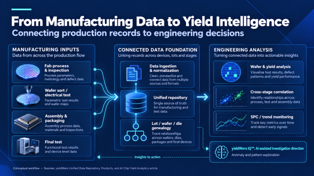
Manufacturing systems collect different pieces of the evidence. Fabrication records describe process conditions and inspected defects. Wafer sort supplies die-level electrical measurements and spatial wafer maps. Assembly logs identify which components went into a package and what equipment handled them. Final-test data reports the completed device’s behavior.
A wafer-edge pattern or localized cluster might suggest where to look, but no spatial signature establishes root cause by itself.
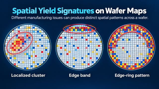
For a multi-die accelerator, those records only become useful together if the manufacturer preserves their relationships. Lot, wafer, and die genealogy lets engineers trace backward from a failed package to individual components, or forward from a suspect wafer lot to every finished product containing its dies. The difficulty increases when data comes from different partners with different formats and unit identifiers.
A yieldWerx customer case study involved a multi-chip product containing four interconnected devices traced across 17 manufacturing stages. The customer needed to connect separate records and identifiers; yieldWerx’s genealogy module allowed engineers to configure the mappings and trace parametric results without custom programming.
Although the case concerns multi-chip semiconductor manufacturing rather than a documented hyperscaler AI accelerator, it demonstrates the kind of problem a heterogeneous AI package can create.
McKinsey’s analysis of end-to-end yield improvement also points to the value of connecting engineering yield losses with their actual manufacturing costs. The payoff shows up in the decisions that follow. If an upstream lot is suspect, which finished accelerators contain its dies? If a process change raises wafer yield, does that improvement survive package assembly and final test?
As custom AI chip production becomes more heterogeneous, answering these questions requires a consistent view of manufacturing history across technologies, facilities, and suppliers.
Having that visibility is one part of the challenge. Making sense of the relationships hidden in thousands of manufacturing and test records is another challenge, especially when engineers are working against production schedules and trying to isolate the source of yield loss.
Also Read: Outlier Detection for Quality Improvement in Semiconductor Testing
Yield Intelligence for a More Distributed Manufacturing Process
Semiconductor manufacturers have spent years developing systems to collect, organize, and analyze production data. As devices become more complex, the value of those systems increasingly depends on how well they connect information from different manufacturing stages and help engineers identify relationships that would otherwise take considerable time to uncover.
A connected data system lets a product engineer compare what happened at wafer fabrication with what appeared at final test. Statistical process control, wafer-level analysis, and defect correlation can then help identify unusual shifts and recurring signatures.
With more complex devices, AI-assisted analysis may help surface candidate relationships sooner, allowing engineers to direct their investigations toward the records most likely to matter. Such methods still require accurate data and engineering validation; a statistical relationship is not automatically a manufacturing cause.
This is where integrated yield analytics and AI-assisted analysis become more relevant.
Also Read: Using AI to Build AI Silicon: How Intelligent Yield Analytics Powers Future-Forward Chip Design
At yieldWerx™, we are developing these capabilities for semiconductor manufacturers. Our existing platform brings manufacturing and test records into a unified environment, supporting yield analysis, device genealogy, and cross-stage correlation.
Take the failing-package example: an engineer used linked records to compare final-test bins with wafer-sort values and assembly history, then narrowed the affected lots and possible process conditions.
The yieldWerx™ IQ™ aims to bring AI-assisted anomaly discovery and pattern investigation deeper into that workflow. The intended benefit is not to replace an engineer’s judgment, but to make unusual relationships easier to surface and prioritize as the manufacturing dataset expands.
For manufacturers working with custom AI silicon, the relevance lies in how devices themselves are changing. Different process technologies, packaging methods, and manufacturing partners produce information that must be interpreted together.
This is especially true for heterogeneous accelerators. Their performance and economics depend on components produced across different processes and suppliers. No single facility has the complete picture by default; connected yield intelligence can help the product team assemble that picture and act on it before avoidable failures spread through production.
Custom Silicon’s Next Test is Manufacturing
Custom AI chips are broadening the semiconductor market because hyperscalers can direct the computing functions they need while specialists supply the expertise to realize them. The decision to commission an ASIC begins with a calculation about workloads, utilization, and long-term cost. It then becomes a set of engineering decisions shared across design partners, foundries, packaging operations, and test facilities.
Those decisions ultimately meet at the finished device. A processor can meet its workload well and still fail to deliver its expected value if qualification takes too long or yield remains unstable.
As heterogeneous integration becomes more common, the companies best able to connect manufacturing history with engineering decisions will be better positioned to bring complex designs into volume production. That is the manufacturing problem behind the industry’s growing interest in yield intelligence and the direction of yieldWerx™ IQ™.
Want to be among the first to see yieldWerx™ IQ™ in action? Schedule a demo with our expert engineering team today.
Frequently Asked Questions (FAQs)
What are custom AI chips?
Custom AI chips are processors developed around selected AI workloads. Many are AI ASICs whose compute, memory, and interconnect architectures are optimized for the applications their developers plan to run at scale.
What is the difference between an AI ASIC and a GPU?
Commercial GPUs are programmable and support a wide range of workloads. Custom AI ASICs can improve efficiency for defined applications, but require substantial investment in design, software, verification, and manufacturing qualification.
When is a custom AI ASIC more economical than a commercial GPU?
When a workload is large and stable enough to recover design, verification, software, and qualification costs, and when the cost per deployable accelerator preserves the expected operating advantage.
Who designs and manufactures hyperscaler AI chips?
Responsibilities differ by program. Hyperscalers may define or own their differentiated architecture, specialists can provide IP and design implementation, and foundries fabricate the dies. Packaging and testing may involve additional partners.
How does custom silicon change semiconductor competition?
It creates additional opportunities for IP providers, design-service firms, foundries, and OSATs, while increasing competition for customer development programs and advanced manufacturing capacity.
Why does advanced packaging make AI chip yield harder to manage?
Individual dies, their interconnects, package assembly, and final qualification must all meet requirements. Problems at any stage can reduce the number of fully functional packages.
Why is manufacturing traceability important for custom AI chip yield?
Traceability connects finished packages to their component dies, wafer lots, manufacturing history, and test results. Those relationships let teams identify common failure causes, determine which material may be affected, and focus corrective action on the relevant stage.