
The ICT sector consumed about 4 percent of global electricity in the use stage, representing about 1.5 to 4 percent of global greenhouse gas (GHG) emissions in 2024.
Modern AI clusters contain thousands of GPUs interconnected by high-speed networks. At these scales, even small improvements in energy efficiency translate into significant reductions in operational cost, cooling requirements, and environmental impact.

This had led to the optical networking industry entering a new phase of design priorities. For decades, network infrastructure was optimized primarily around capacity, reach, and latency. Today, however, another parameter has become equally critical: power consumption efficiency.
The focal point of this shift is picojoules per bit (pJ/bit)—a critical efficiency metric that measures the energy required to move a single bit of data across a network element or fiber link. Though it appears as a singular value, it represents the collective performance of the entire hardware stack, from the high-speed Digital Signal Processor (DSP) and laser sources to the optical amplifiers and thermal management systems that keep them operational.
Optical networking already forms the backbone of global connectivity, carrying the vast majority of inter-data-center and long-haul traffic. But as bandwidth requirements continue to rise—from 400G links to 800G and soon 1.6T—the industry must carefully measure and optimize the power consumed by every bit of transmitted data.
This article provides a practical guide to understanding:
- Why power efficiency matters in optical networks
- The metrics used to measure energy efficiency
- Tools and methodologies used to evaluate power consumption, and
- Emerging trends in optical networking technology that design engineers can apply to reduce energy usage without compromising performance.
Learn how yieldWerx helps teams analyze test data to improve yield, reliability, and power efficiency.
Two Decades of Efficiency: The Road to Sub-Single-Digit pJ/bit
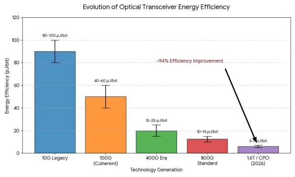
Over the last twenty years, the optical industry has achieved a monumental 10-fold increase in energy efficiency. This leap is driven by the synergy of CMOS scaling, photonic integration, and advanced DSP algorithms. It has allowed each new generation of transceivers to multiply capacity while simultaneously slashing the energy cost per bit.
The efficiency roadmap highlights a dramatic descent in power consumption:
- 10G Legacy: Early direct-detect transceivers set the baseline at 80–100 pJ/bit.
- The Coherent Shift (100G): The move to DP-QPSK modulation and 40nm nodes cut requirements nearly in half, to 40–60 pJ/bit.
- The 400G Era: By leveraging 7nm CMOS and higher-order modulation, efficiency improved to the 15–25 pJ/bit range.
- The Modern 800G Standard: Utilizing 5nm DSPs, current pluggable modules operate at 10–15 pJ/bit.
- The Leading Edge (2026): Production Co-Packaged Optics (CPO) have now broken the 7 pJ/bit barrier, while the first 1.6T transceivers on 3nm processes are beginning to deploy, pushing efficiency into the single digits.
Understanding Power Metrics in Optical Networks
Optimizing energy efficiency begins with the ability to measure power consumption accurately and consistently. In optical networking, engineers use several standardized metrics to evaluate how efficiently network components convert electrical energy into data transmission capacity.
Energy per Bit (pJ/bit)
The most important metric for evaluating optical network efficiency is energy per bit, typically expressed in picojoules per bit (pJ/bit). This metric quantifies the amount of energy required to transmit one bit of data through a device or network segment.
The formula is straightforward:
Where:
Ptotal = power consumption of the device
RData = data rate
For example, if a 400G optical transceiver consumes 20 W, the energy efficiency is approximately 50 pJ/bit.
This metric allows engineers to compare devices across generations. Even if a higher-speed module consumes more absolute power, it may still be significantly more efficient because its power overhead is spread across more data throughput. For instance, a single 400G transceiver is generally more energy efficient than four 100G modules, because the fixed power components—lasers, packaging, and cooling—are shared across a higher data rate.
The industry has made substantial progress using this metric. Early optical modules often exceeded 80–100 pJ/bit, while modern systems aim for single-digit pJ/bit efficiency.
Bandwidth Density (Tbps/mm or Tbps/W)
Bandwidth density measures how much data throughput an optical system can deliver relative to physical area or power consumption. In modern optical networking—especially in hyperscale data centers—this metric has become critical because both space and power are limited resources.
Bandwidth density is typically expressed in two forms:
- Tbps/mm² – throughput per unit of physical chip or module area
- Tbps/W – throughput delivered per watt of power
Higher bandwidth density means a system can move more data using less hardware and less energy. Traditional pluggable optical modules sit at the front panel of switches and require electrical signals to travel longer distances inside the switch ASIC package. This increases power consumption, signal loss, and thermal load.
Co-packaged optics, by contrast, place optical engines directly next to the switching silicon, dramatically shortening electrical paths. This enables:
- higher throughput per switch
- reduced electrical I/O power
- better thermal and space utilization inside networking equipment
Optical Power Efficiency (dBm and Optical Link Budget)
In optical communication systems, maintaining sufficient signal power across the fiber link is essential for reliable data transmission. Optical power efficiency is evaluated through parameters such as:
- Optical launch power – the signal power emitted by the transmitter
- Receiver sensitivity – the minimum optical power required for the receiver to correctly detect the signal
- Optical link budget – the total allowable loss across the link
The link budget is typically calculated as:
Link Budget = Tx Power − Rx Sensitivity
This value represents the maximum total loss the system can tolerate while still maintaining reliable communication.
Losses within a link can come from several sources like:
- fiber attenuation
- connectors and splices
- optical filters and switches
- dispersion and other signal impairments
Efficient optical power management ensures that the transmitted signal is strong enough to maintain reliability but not excessively high, which would require additional power consumption or unnecessary amplification.
Optimizing the link budget allows operators to design systems that balance performance, reach, and energy efficiency.
Bit Error Rate (BER) and Power Efficiency
Although the Bit Error Rate (BER) is primarily a reliability metric rather than a direct energy metric, it plays an important role in power optimization.
BER measures the proportion of transmitted bits that are incorrectly received. High-performance optical systems typically aim for:
BER < 10-9
Maintaining a low BER ensures that the transmitted signal remains sufficiently clear and detectable by the receiver.
If the optical signal becomes too weak or distorted, the system must rely more heavily on digital signal processing (DSP) and forward error correction (FEC) to recover the data. While these techniques improve reliability, they also increase:
- DSP power consumption
- processing latency
- system complexity
Optimizing optical power levels, modulation formats, and receiver sensitivity helps maintain low BER while minimizing the computational overhead required for error correction.
In practice, achieving the optimal balance between signal strength, energy efficiency, and error performance is one of the key challenges in modern optical network design.
Tools And Strategies Used to Measure Power Optimization in Optical Networks
Unlike traditional fiber-optic systems where optical power is typically measured externally, PICs rely on integrated monitoring structures and telemetry systems that provide continuous visibility into signal behavior within the chip.
Optical power in photonic systems is typically expressed in dBm, a logarithmic unit referenced to one milliwatt. Because optical signals experience attenuation as they pass through modulators, splitters, filters, and waveguides, monitoring power levels is essential for maintaining signal integrity and ensuring that receivers operate within their sensitivity range.
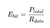
Waveguide Tap Couplers
Inside a PIC, optical power is commonly measured using waveguide tap couplers and integrated photodiodes. Tap couplers divert a very small fraction of the optical signal—usually between one and five percent—from the main waveguide. This sampled light is routed to an integrated photodiode, which converts the optical signal into an electrical current proportional to the optical power. Because only a small portion of the signal is tapped, the monitoring process introduces minimal additional loss.
These on-chip sensors feed data into telemetry systems, which allow network operators and control software to monitor optical performance in real time. Telemetry can report parameters such as transmitted optical power, received optical power, laser bias current, device temperature, and power efficiency. In large-scale optical systems, this data is used for digital diagnostics monitoring (DDM) and automated network management, helping operators detect power imbalances, component drift, or early signs of device degradation.
Traditional Methods
During development and manufacturing, engineers also rely on specialized test equipment to measure and optimize optical power more precisely. Optical power meters provide calibrated absolute power measurements, optical spectrum analyzers reveal wavelength and power distribution, and bit-error-rate testers (BERTs) help correlate optical power levels with overall link reliability. These tools are essential for validating link budgets and calibrating on-chip monitoring circuits.
Strategies for Reducing Energy per Bit in Optical Networks
Achieving lower energy consumption requires improvements across several parts of the optical system, including digital processing, photonic integration, amplification, and network architecture.
More Efficient DSPs and Advanced Semiconductor Processes
The digital signal processor (DSP) is typically the largest power consumer in a coherent optical transceiver. Improvements in semiconductor manufacturing have played a major role in reducing this power consumption.
Each transition to a more advanced CMOS process node—from 16 nm to 7 nm, then to 5 nm and now 3 nm—reduces switching power in the DSP thanks to lower supply voltages and smaller transistors. As of 2026, many 800G coherent DSPs are manufactured using 5 nm technology, while 3 nm designs are beginning to appear in 1.6T systems.
Industry roadmaps aim to push DSP efficiency below 5–6 pJ/bit by the end of the decade, supported by both semiconductor scaling and smarter algorithms. Improvements in forward error correction (FEC), signal equalization, and carrier recovery techniques can reduce the number of operations required to process each bit of data, directly lowering power consumption.
Another promising approach is rate-adaptive transmission, where DSP power can be reduced by lowering the symbol rate during periods of lower traffic demand.
Photonic Integration and Silicon Photonics
Another major contributor to energy efficiency is photonic integration, where multiple optical components are combined onto a single chip.
Photonic Integrated Circuits (PICs) reduce the size, cost, and power consumption of optical systems by integrating components such as modulators, photodetectors, and polarization-handling elements. Several integration platforms are used in modern optical transceivers.
Indium phosphide (InP) PICs can integrate lasers, modulators, and detectors on a single chip, making them attractive for high-performance coherent systems where laser quality is critical.
Silicon photonics (SiPh) has become the dominant platform for large-scale optical interconnects. Because it uses CMOS-compatible manufacturing processes, silicon photonics benefits from large wafer sizes, high yields, and lower costs. As of 2026, shipments of silicon photonics-based 800G modules exceed seven million units annually, and industry projections suggest that around 44% of optical transceivers will use silicon photonics by 2028.
Integration also improves energy efficiency. By placing optical components on a single chip, silicon photonics eliminates many discrete electrical connections and their associated losses.
Rate-Adaptive Transmission for Energy Savings
Modern optical networks are increasingly adopting elastic transmission technologies that can adapt to traffic conditions.
In Elastic Optical Networks (EONs), transceivers can adjust both the modulation format and symbol rate depending on link requirements and traffic demand. During periods of lower traffic, reducing the transmission rate allows the DSP and other components to operate at lower power.
Studies show that lowering the symbol rate can reduce DSP power consumption by up to 40%, while network-level simulations demonstrate energy savings of more than 30% when networks dynamically adjust transmission rates to match daily traffic patterns.
System-Level Approaches to Green Optical Networks
While component improvements are important, the largest gains often come from architectural changes at the system level.
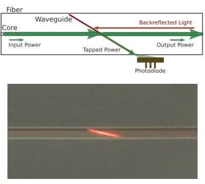
Co-Packaged Optics (CPO)
One of the most significant architectural shifts in data center networking is co-packaged optics (CPO).
In traditional systems, pluggable optical modules sit at the front panel of a switch, requiring high-speed electrical signals to travel across long copper traces from the switch ASIC to the module. These long electrical paths increase signal loss and require additional electronics such as retimers.
CPO places optical engines directly next to the switching ASIC inside the same package, dramatically shortening the electrical path from centimeters to millimeters. This reduces electrical losses, eliminates retimer chips, and lowers overall power consumption.
Current CPO implementations achieve around 5–7 pJ/bit, compared with roughly 15 pJ/bit for traditional pluggable optics. For a high-capacity switch with dozens of optical ports, this improvement can translate into hundreds of watts of power savings.
Read More About Silicon Photonics & CPOs in Our Separate Blog Posts:
Bright Horizons in Silicon Photonic
Understanding Co-Packaged Optics: The Need for Integrating Photonics and Chiplets
AI-Driven Network Energy Optimization
Artificial intelligence is increasingly being used to optimize energy usage across large optical networks.
Machine learning systems can analyze network conditions in real time and automatically adjust transmission parameters such as modulation format, launch power, and wavelength routing. AI-based traffic engineering can also consolidate traffic onto fewer active links during low-demand periods, allowing unused equipment to be powered down.
Early network deployments have shown energy savings of around 20% or more using AI-driven optimization without compromising service quality.
Power-Aware Network Design
Energy efficiency can also be improved through smarter network planning and architecture.
For example, optimizing the placement of optical amplifiers can reduce the number of amplification sites along a fiber route. Choosing modulation formats that balance spectral efficiency with DSP power consumption can also lower energy usage.
Another important trend is IP-over-DWDM networking, where routers and switches directly interface with DWDM optical wavelengths without intermediate transponder systems. Technologies such as 400G ZR and ZR+ coherent pluggables make this approach practical, reducing both equipment complexity and power consumption.
Case Study: NVIDIA AI Data Centers — Co-Packaged Optics for GPU Fabrics
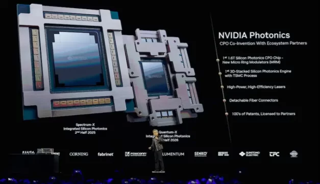
One of the clearest real-world examples of power optimization in optical networking comes from AI data center infrastructure, where hyperscale GPU clusters require extremely high bandwidth interconnects. As AI training workloads grow larger, the energy required to move data between GPUs has become a major operational constraint.
At GTC 2025, NVIDIA introduced next-generation networking platforms that integrate co-packaged optics (CPO) directly into switching ASICs used in its Spectrum-X Ethernet and Quantum-X InfiniBand switches. This architectural shift is designed to overcome the power and bandwidth limitations of traditional pluggable optical modules used in AI clusters. They integrate optics innovations with 4x fewer lasers to deliver 3.5x more power efficiency, 63x greater signal integrity, 10x better network resiliency at scale and 1.3x faster deployment compared with traditional methods.
In large hyperscale AI clusters, interconnect energy consumption can be enormous. NVIDIA estimates that transitioning from pluggable optics to co-packaged optics can dramatically reduce networking power requirements.
Conclusion
Energy efficiency has become a defining challenge for modern optical networking infrastructure. As global data demand continues to rise and AI workloads reshape data center architectures, the industry must carefully balance bandwidth, latency, and power consumption.
Metrics such as pJ/bit provide a practical framework for evaluating network efficiency, while advanced measurement tools and system-level modeling techniques help engineers identify opportunities for optimization.
However, measuring power efficiency is only the first step. Achieving meaningful improvements requires the ability to correlate performance data across the entire hardware lifecycle—from wafer fabrication and photonic device manufacturing to system-level testing and field deployment. As optical systems become more complex, with tightly integrated photonic and electronic components, identifying sources of power inefficiency increasingly depends on advanced data analytics and yield intelligence.
This is where platforms like yieldWerx play an important role. By aggregating and analyzing large volumes of semiconductor test, manufacturing, and reliability data, such platforms enable engineering teams to detect performance anomalies, optimize device yields, and improve power efficiency across optical components and photonic integrated circuits.
In the years ahead, the ability to deliver more bandwidth with fewer watts will become one of the most important benchmarks for optical networking performance. Achieving this goal will depend not only on innovations in photonics and semiconductor design, but also on the data-driven manufacturing intelligence needed to continuously optimize the performance of complex optical systems at scale.
Ready to unlock deeper insights into power efficiency and device performance? See how yieldWerx helps semiconductor and photonics teams turn complex test data into actionable yield and reliability improvements