The future of quantum computing may be built on light, but building reliable photonic quantum hardware is anything but simple. Every team developing a quantum chip eventually faces the same three-way engineering decision:
Which photon source should we use?
Which detector provides the best performance?
And which photonic platform offers the right balance of scalability and manufacturability?
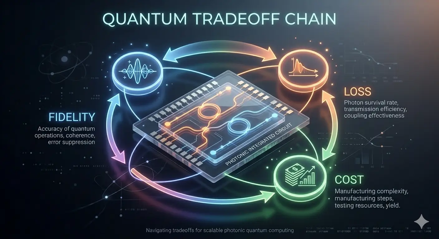
Ultimately, quantum design becomes a balancing act between three competing objectives:
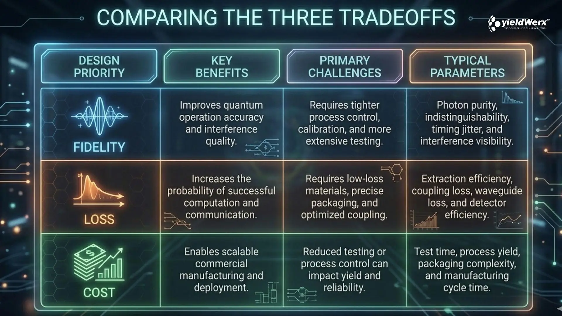
- Fidelity: How accurately can the system generate, manipulate, and detect quantum information?
- Loss: How many photons survive from source to measurement?
- Cost: How much testing, integration, and manufacturing complexity can the architecture support and still produce sufficient business profits?
This “quantum tradeoff chain” is increasingly shaping the future of photonic device manufacturing and overall photonics yield optimization strategies. Overall, quantum systems are highly sensitive, and obtaining more information about them requires more measurements, more specialized infrastructure, and more complex data analysis. Unfortunately, all of which increases cost.
In this article, we will explore the fundamental tradeoff chain that every photonic quantum hardware team must navigate. We’ll examine how photonic yield analytics will play a critical role in scaling quantum photonics from the lab to the foundry.
Why the Tradeoff Exists
Unlike classical electronic systems, quantum information cannot simply be amplified or regenerated if errors occur. In photonic quantum computing, every lost or degraded photon directly impacts the probability of completing a computation.
At the same time, improving quality often means adding more testing, tighter process controls, and more sophisticated packaging and calibration steps. As in semiconductor manufacturing, additional inspection and validation can improve yield and reliability. However, they also increase cost and cycle time.
The difference is that quantum photonic systems operate with far tighter margins. The challenge is not just making a device that works beyond laboratories; it is making one that can be manufactured repeatedly while preserving extremely high optical performance.
Achieving this level of scalable performance requires a robust underlying infrastructure. To learn more about how this works at scale, see our deep dive on Scaling Quantum Systems With Photonic Interconnects and Quantum Key Distribution
Fidelity: How Much Interference Quality Is Enough For Quantum Networks?
Recent advances have pushed two-photon interference visibility to 92% for C-band and single-photon purity and indistinguishability beyond 98%.
Fidelity describes how accurately the hardware performs its intended quantum operation. In practical terms, this means generating photons that are as identical as possible, maintaining stable interference, and ensuring detectors produce accurate measurement outcomes.
A useful analogy is active noise-cancelling headphones, where carefully engineered sound waves interfere with incoming noise to reduce background sound. Similarly, identical photons can interfere with one another to produce unique quantum effects necessary for quantum networking and quantum computing.
Small variations can have outsized effects. A slight drift in wavelength, polarization, or timing can reduce interference visibility and increase computational error rates. Similarly, detector timing jitter or packaging-induced alignment shifts can gradually degrade system performance.
For example, researchers recently demonstrated quantum interference between single photons transmitted over more than 300 km of optical fiber. For the photons to interfere successfully, their wavelength, timing, and other properties had to be nearly identical. Even small mismatches can reduce interference visibility, making it more difficult to reliably transmit quantum information over long distances.
Achieving high fidelity often requires:
- Deterministic single-photon sources.
- Ultra-low-noise single-photon detectors.
- Tight optical alignment tolerances.
- Stable integrated photonic circuits.
- Extensive optical characterization and validation.
For photonic quantum hardware, the answer is application-dependent. A laboratory prototype may tolerate manual calibration and extensive optical testing. A commercial system manufactured at scale cannot.
Loss: The Hidden Barrier to Scalability
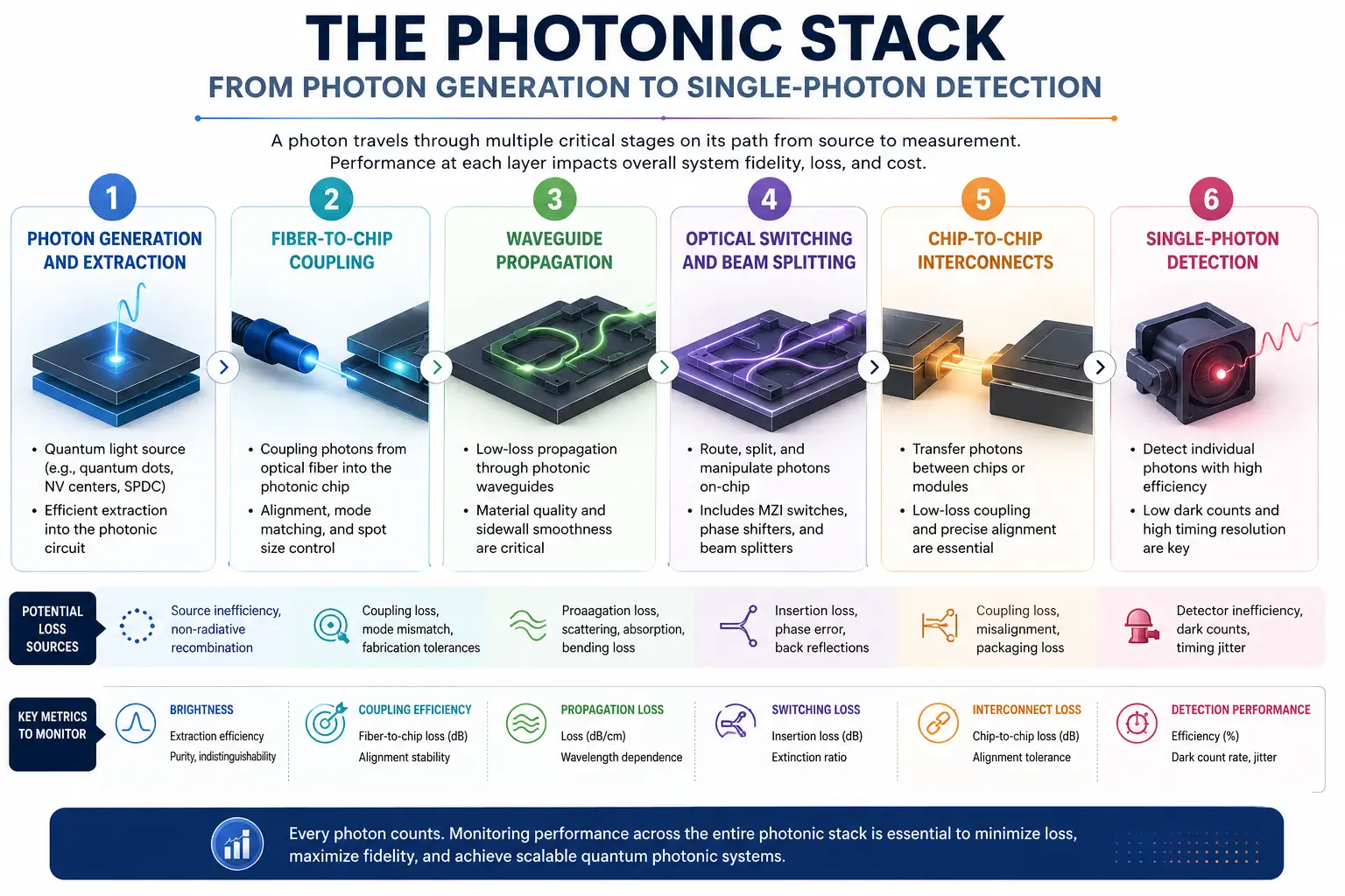
Loss occurs at every stage of the photonic stack. Unlike classical communication systems, lost quantum information cannot be simply amplified because of the fundamental no-cloning principle. Every missing photon reduces the probability of a successful operation.
This is why low-loss photonic integration has become such a major research focus. Recent demonstrations of deterministic quantum-dot photon sources with system efficiencies exceeding 70% represent an important milestone because they move beyond the theoretical loss-tolerance threshold needed for scalable architectures.
However, reducing loss is rarely free. Lower-loss materials, improved packaging, tighter process controls, and more comprehensive optical testing all add cost and manufacturing complexity. In many cases, the engineering challenge is not eliminating loss entirely—it is determining how much loss can be tolerated while maintaining acceptable fidelity without making the product economically impractical.
Cost: The Often-Overlooked Quantum Metric
A modern photonic quantum system may integrate hundreds of optical components, multiple material platforms, cryogenic detectors, precision packaging, and advanced semiconductor manufacturing processes.
Cost is therefore not simply the price of a chip. It is the cumulative impact of:
- Specialized quantum materials.
- Hybrid integration of multiple photonic platforms.
- Precision optical alignment.
- Cryogenic infrastructure.
- Test and inspection time.
- Packaging complexity.
- Yield losses during manufacturing.
There is a direct relationship between testing and cost. More test coverage improves confidence in performance and catches latent defects before shipment, but every additional measurement increases production time and operational expense.
“There’s this constant balance that has to occur,” says Keith Schaub, vice president of technology and strategy at Advantest. “We need to apply the budget to get as much test coverage as we can at the best quality for that budget. That’s where the challenge is.”
This tradeoff is already familiar in advanced semiconductor manufacturing. Test escapes increase field failures, while excessive testing drives up the cost of goods sold. Photonic quantum hardware amplifies this challenge because the devices themselves are inherently more sensitive to small process variations.
A slight deviation in waveguide geometry, coupling efficiency, or detector alignment may have little impact in a classical optical transceiver, but it can significantly reduce the fidelity of a quantum operation.
The result is a new optimization problem: balancing sufficient test coverage to guarantee performance while minimizing unnecessary manufacturing overhead.
Comparing the Three Tradeoffs
The Source, Detector, and Platform Decision
The fidelity-loss-cost tradeoff is ultimately expressed through three fundamental hardware choices.
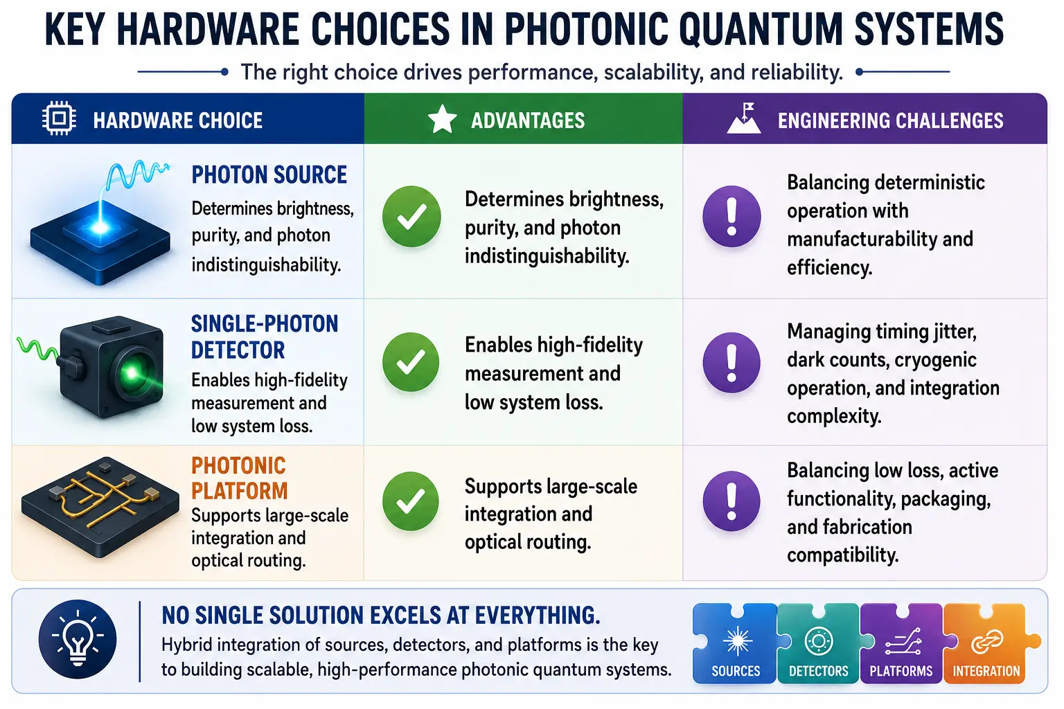
No single material platform excels across all categories.
Silicon photonics offers mature manufacturing and scalability. Quantum-dot platforms provide on-demand single-photon generation. Lithium niobate enables high-speed electro-optic switching. Superconducting detectors deliver industry-leading sensitivity but introduce cryogenic requirements.
As a result, many next-generation architectures are moving toward hybrid integration, combining the strengths of multiple technologies while minimizing their individual limitations.
Silicon Photonics Analytics: Leading The Shift from Quantum Physics to Quantum Manufacturing
The central challenge has shifted from proving that a quantum device works to proving that it can be manufactured repeatedly and economically.
During a panel discussion at SPIE Advanced Lithography Conference, executives from PsiQuantum, Google, and IBM highlighted a common theme: the future of quantum computing will depend as much on semiconductor manufacturing as on quantum physics itself.
While different quantum architectures have different requirements, they all demand extraordinary levels of process control and consistency. As Mark Thompson of PsiQuantum noted, “Small improvements in qubit performance can lead to huge improvements in system performance,” emphasizing how even nanometer-scale process variations can have an outsized impact on photonic quantum hardware.
At the same time, IBM’s Markus Brink pointed out that today’s quantum systems already depend heavily on conventional semiconductor technology, observing that, “We rely on CMOS technology.”
Together, these perspectives reinforce a broader industry trend: as quantum hardware scales, advances in process control, precision manufacturing, and semiconductor infrastructure will become just as critical as breakthroughs in quantum device design.
The industry is increasingly adopting a foundry-style model, where repeatability, yield, and process control become just as important as breakthrough device performance. In this environment, the tradeoff becomes a data problem.
This is where optical test data analysis and integrated photonics yield analytics become increasingly important.
The same data-driven approaches that transformed semiconductor manufacturing are beginning to shape the future of quantum chips, enabling engineers to identify process excursions, correlate optical performance with manufacturing parameters, and optimize yield across increasingly complex integrated photonic systems.
The Bottleneck: Why Quantum Chip Testing Defies Classical Methods?
Unlike classical semiconductor devices, quantum chips cannot be evaluated using simple pass/fail methods because the act of measuring a quantum system can alter its behavior. Therefore, achieving high fidelity while controlling manufacturing cost requires balancing extensive characterization with practical production constraints.
Some of the biggest challenges include:
Fragile Quantum States:
Quantum information is highly sensitive to environmental disturbances. Small fluctuations in temperature, electromagnetic interference, optical alignment, or mechanical vibrations can introduce errors or degrade performance.
Specialized Test Environments:
Many quantum architectures operate under extreme conditions, including cryogenic temperatures and ultra-low-noise environments. Testing and validation require sophisticated infrastructure and tightly controlled operating conditions.
Statistical and Repetitive Measurements:
Quantum measurements are inherently probabilistic, meaning a single observation provides limited information. Engineers often need to perform thousands of repeated measurements to accurately characterize device behavior and estimate error rates.
Data Volume and Analytics Complexity:
Modern quantum test flows generate enormous amounts of measurement data across multiple operating conditions, calibration cycles, and manufacturing lots. Extracting meaningful insights requires advanced optical test data analysis, capable of identifying subtle patterns such as timing jitter, optical performance drift, device-to-device variability, and process-induced correlations that may only emerge over thousands or millions of measurements.
Scaling and Crosstalk:
As systems integrate larger numbers of qubits or photonic components, interactions between neighboring devices become increasingly difficult to isolate. Crosstalk, synchronization issues, and complex multi-device dependencies make calibration and verification more challenging.
These challenges create a direct connection between fidelity, loss, and cost tradeoff. More testing and characterization improve confidence in device quality and long-term reliability, but they also increase data volumes, manufacturing complexity, and overall production costs.
Finding the Right Balance
As Val Zwiller and colleagues wrote, “Building a desired hybrid integrated quantum photonic device requires a trade-off between achieving the best performance of a specific element and its potential for hybrid integration. “
The goal of photonic quantum engineering is not to eliminate every source of loss or perform every possible test. It is to identify the point where fidelity is high enough, losses are low enough, and manufacturing costs remain practical for scalable production.
That balance will not be determined by a single breakthrough device or a single material platform. It will be achieved by understanding the relationship between design choices, process variation, and measurable manufacturing data.
Organizations that can effectively connect optical performance metrics with manufacturing analytics will be better positioned to improve yield, reduce variability, and accelerate the transition from promising laboratory prototypes to reliable commercial systems.
The path to scalable quantum computing may ultimately depend not only on building better photonic devices, but on building better insight into the data those devices generate throughout the manufacturing process.
FAQs
What is interference in quantum computing? Is it good or bad?
Quantum interference occurs when identical quantum particles, such as photons, interact and their probability waves combine. It is a fundamental and beneficial phenomenon that enables quantum computers to amplify correct outcomes and suppress incorrect ones.
Why are qubits so fragile?
Qubits are highly sensitive because they exist in delicate quantum states called superposition and entanglement. Small disturbances from heat, electromagnetic noise, or vibrations can disrupt these states and introduce errors.
What are quantum dots?
Quantum dots are tiny semiconductor nanostructures that behave like artificial atoms. In photonic quantum computing, they can generate single photons on demand, making them promising building blocks for scalable quantum systems.
How is a quantum chip different from a conventional semiconductor chip?
Conventional chips process information using classical bits that are either 0 or 1. Quantum chips use qubits, which can exist in multiple states simultaneously and exploit quantum effects such as superposition and entanglement, requiring far more precise control and testing.
What are the top companies in the quantum computing space?
Some of the leading companies include IBM, Google, PsiQuantum, IonQ, Quantinuum, Rigetti Computing, Xanadu, and Alice & Bob, each pursuing different quantum hardware approaches.
What is lithium niobate and why is it so useful?
Lithium niobate (LiNbO₃) is a crystalline material with exceptional electro-optic properties. It enables ultra-fast optical modulation and switching, making it a key material for photonic integrated circuits and next-generation quantum communication systems.
Why are silicon photonics and photonic integrated circuits so crucial for quantum computing?
Silicon photonics and photonic integrated circuits (PICs) allow optical components such as waveguides, modulators, and couplers to be integrated onto a single chip using semiconductor manufacturing techniques. This enables lower cost, higher scalability, and a practical path toward foundry-scale photonic quantum hardware.
What is C-Band?
The telecommunications C-band is a range of infrared wavelengths centered around 1550 nanometers (nm), where optical fiber experiences its lowest signal loss. Because existing global fiber-optic networks are optimized for this wavelength, many photonic quantum technologies aim to operate in the C-band to enable long-distance, high-efficiency quantum communication.