LiDAR has become a critical sensing modality in advanced driver assistance systems (ADAS) and autonomous vehicles, where accurate, real-time perception of the environment is essential for safe operation. While system architectures have matured rapidly, achieving consistent performance in real-world conditions remains challenging due to sensitivity to environmental factors such as ambient light, surface reflectivity, and contamination. As LiDAR designs evolve toward photonic integration, performance limitations increasingly shift away from macro-scale optical design and toward the behavior, variability, and calibration of underlying photonic components. In this context, testing and calibration of photonic integrated circuits (PICs) become central to system-level performance optimization rather than post-design validation steps.
What Is LiDAR as a Photonic Sensing System?
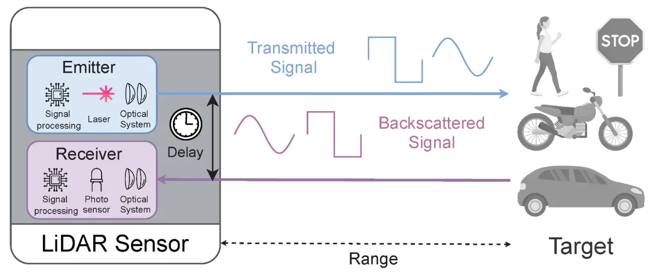
LiDAR, short for Light Detection and Ranging, is a remote sensing technology that uses laser light to measure distances and generate precise three-dimensional maps of its surroundings. It works by emitting rapid pulses of light and calculating how long they take to reflect back from objects, allowing the system to determine position, shape, and motion with high accuracy.
Because LiDAR relies entirely on the generation, manipulation, transmission, and detection of light, it is fundamentally a photonic system. In fact, it is often described as a photonic equivalent of radar, where optical components such as lasers, waveguides, and photodetectors enable high-resolution sensing and beam steering capabilities.
Modern silicon photonics platforms allow dense integration of optical components using the same scalable, high-yield techniques developed for the electronics industry. This enables LiDAR systems to achieve smaller size, lower power consumption, and reduced cost, while maintaining high performance.
In this article we will be focusing predominantly on solid-state LIDARs that rely on beam steering principles rather than legacy mechanically rotating systems.
Scaling Challenges in Photonic LiDAR Sytems
LiDAR systems are currently at an inflection point where architectural maturity and integration progress coexist with increasing challenges in performance consistency at scale. While design methodologies and system benchmarks are well established, reliable scaling across high-channel-count photonic systems remains a limiting factor.
That challenge is scaling performance reliably across increasingly complex photonic systems.
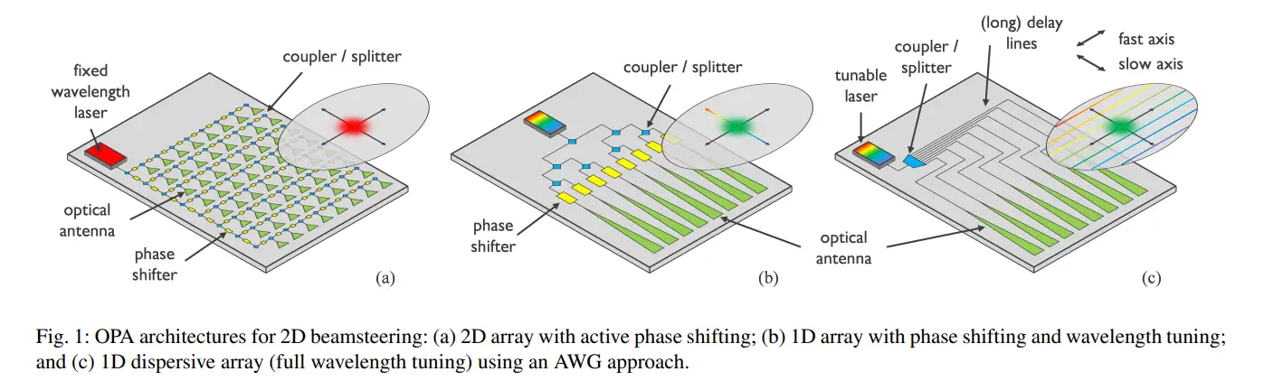
At the center of this challenge are Photonic Integrated Circuits. These devices enable solid-state LiDAR by integrating lasers, modulators, phase shifters, and waveguides onto a single chip. In optical phased array architectures, they allow beam steering without moving parts, making them ideal for automotive and industrial applications.
However, this integration comes at a cost. As channel counts increase into the hundreds or even thousands, PICs become systems where small physical variations translate into measurable performance deviations.
PIC Architecture: A High-Dimensional Optical System
A LiDAR PIC is not a simple circuit. It is a dense optical network composed of interconnected signal paths.
Waveguides route light across the chip. Splitters distribute signals into multiple channels. Phase shifters control interference patterns to steer beams. Modulators encode information onto optical carriers. In some architectures, detectors are also integrated.
Each of these components introduces variability. Even at the fabrication level, differences in waveguide width or refractive index can alter optical propagation. In high-channel-count optical phased arrays, maintaining phase coherence across channels becomes particularly challenging.
Research shows that even in relatively modest systems, such as 128-channel or 256-channel OPAs (Optical Phase Arrays), precise phase control and calibration are required to achieve acceptable beam quality and steering accuracy.
This complexity transforms the PIC into a high-dimensional system where performance emerges from the interaction of many variables rather than any single parameter.
This is where testing and calibration move from validation tasks to core system capabilities.
Multi-Stage Testing: Building a Complete Picture of Performance
Wafer-Level Testing: Establishing the Electro-Optical Baseline
Wafer-level testing is where the intrinsic behavior of a LiDAR SoC is first understood. At this stage, the chip is still un-packaged, allowing engineers to probe both its electrical and optical characteristics in a highly controlled environment.
Beyond standard parametric checks, the focus is on validating timing precision, detector response, and early optical behavior using hybrid electrical and optical probing setups.
What makes this stage unique is the scale and granularity of data. With thousands or even millions of sensing elements per die, wafer testing generates dense datasets that capture performance variation across both the chip and the wafer. These measurements are mapped spatially to uncover process-driven patterns and to identify known good die.
More importantly, wafer-level results form the foundation for calibration and yield learning, serving as the first “fingerprint” of how each device is likely to behave downstream.
Assembly-Level Testing: Validating Integration and Alignment
Once the chip is packaged, testing shifts from intrinsic behavior to integration quality. Assembly introduces new variables—parasitics, thermal effects, and most critically, optical alignment. Then, the LiDAR SoC is evaluated in conditions that more closely resemble its final form, with emitters, detectors, and optical paths interacting as a cohesive unit.
Engineers re-verify electrical performance under packaging constraints while also validating end-to-end optical signal flow. Subtle misalignments or coupling losses that were invisible at wafer level can now impact system efficiency and accuracy.
This stage also includes final calibration steps, where device-specific adjustments are applied to account for packaging-induced variation. The result is a more complete understanding of how the chip performs as part of a physical subsystem.
System-Level Testing: Proving Real-World Performance
System-level testing is where the LiDAR SoC is evaluated as part of a fully integrated module operating in realistic conditions. The emphasis moves to end-to-end performance—how accurately and consistently the system can detect, measure, and reconstruct its environment.
Through controlled scenarios that simulate real-world use cases, engineers assess distance accuracy, point cloud quality, and dynamic behavior under varying conditions such as motion, lighting, and temperature. This stage also serves as the final point of correlation, linking earlier test data to actual system outcomes.
By the end of system-level validation, the LiDAR device is no longer just a collection of components, but a complete sensing system ready for deployment.
The Data Explosion: From Measurement to Complexity
One of the least discussed challenges in PIC-based LiDAR is the scale of data generated during testing.
Each channel produces multiple measurements across wavelength, voltage, temperature, and time. When multiplied across hundreds of channels and multiple test stages, the result is a combinatorial explosion of data.
This is not just large datasets. It is high-dimensional data, where relationships between variables are often nonlinear and interdependent.
Research into high-channel-count OPAs highlights the difficulty of calibrating and characterizing such systems, noting that calibration complexity grows rapidly with channel count and coupling effects.
Without structured analytics, much of this data remains underutilized. The challenge is not just measurement, but also interpretation.
What is LIDAR Calibration? The Core Mechanism for Performance Control
LiDAR calibration ensures that all components of the system operate in precise coordination to capture accurate data. This process involves aligning key elements such as the laser scanner, GNSS unit, and IMU so that the resulting 3D point clouds faithfully represent the real-world environment.
In applications like aerial mapping, autonomous navigation, and surveying, even small calibration errors can introduce distortions in the data, ultimately impacting analysis, decision-making, and overall project outcomes.
What is a Calibration Curve?
A LiDAR calibration curve is not a single curve, but a set of relationships that map internal signals to real-world measurements. The most fundamental example is the relationship between measured signal (such as beat frequency in FMCW systems) and actual distance, which is ideally linear but often requires correction due to noise, drift, and system nonlinearity.
In photonic LiDAR systems, additional calibration curves become critical. These include mappings between control signals and phase shifts for beam steering, optical power and detection sensitivity, and wavelength tuning and system stability. Because these parameters are tightly coupled, calibration is not a one-time adjustment but an ongoing process that ensures accuracy across devices and operating conditions.
In optical phased arrays, calibration is primarily concerned with aligning phase across channels to achieve coherent beamforming. However, it also extends to power balancing, spectral correction, and compensation for loss and crosstalk.
Traditional approaches often rely on sequential tuning of individual elements. However, this becomes inefficient as system size increases. Errors can propagate, and interactions between components make independent calibration difficult.
Recent research has explored more advanced techniques, including:
- Global calibration strategies that treat the PIC as a system
- Optimization algorithms such as genetic algorithms for high-channel arrays
- Machine learning models that capture nonlinear relationships between control signals and optical outputs
These approaches reflect a shift from component-level correction to system-level optimization.
Environmental and Dynamic Calibration
Static calibration is not sufficient for LiDAR systems operating in real-world environments.
Temperature-induced phase drift is a well-known issue in silicon photonics. Even small temperature changes can shift optical phase, altering beam direction and degrading accuracy. Research has demonstrated the need for adaptive beamforming techniques that maintain performance across temperature variations.
Dynamic calibration strategies address this by incorporating feedback mechanisms and real-time adjustment. These systems continuously monitor performance and apply corrections, effectively turning calibration into an ongoing process rather than a one-time step.
Automating Calibration at Scale
As PIC complexity grows, automation becomes essential.
Manual calibration is not feasible when dealing with hundreds of channels and multiple interacting parameters. Automated systems integrate calibration into test workflows, enabling high-throughput adjustment during manufacturing.
More advanced approaches embed calibration into system operation. Some of them are:
Closed-loop feedback systems use on-chip monitors and photodetectors to continuously measure performance and correct phase, power, and alignment in real time.
Lookup tables (LUTs) map control inputs like current or voltage to calibrated outputs, enabling fast, repeatable corrections during operation.
Machine learning models capture nonlinear relationships across many channels, allowing simultaneous, scalable calibration in high-density PIC systems.
On-chip self-calibration structures such as tap couplers and monitoring photodiodes enable devices to measure and adjust their own behavior.
This transforms calibration from a production bottleneck into a scalable capability.
Conclusion: Testing and Calibration Define the Limits of LiDAR
The trajectory of LiDAR development continues toward higher integration density, increased channel counts, and more demanding performance requirements.
Within this progression, the primary differentiator is no longer system architecture alone, but the ability to measure complex photonic behavior, interpret high-dimensional test data, and maintain performance through continuous calibration.
PIC testing and calibration are not peripheral activities. They define how well a system performs, how reliably it can be manufactured, and how effectively it can operate in the real world.
In the end, the question is not whether you can build a LiDAR system.
It is whether you can control it.
The challenge of interpreting high-dimensional test data is where advanced yield analytics platforms become critical.
Solutions like yieldWerx are designed to ingest, normalize, and analyze large-scale semiconductor and photonic test datasets across wafer, assembly, and system-level stages. By correlating electrical, optical, and parametric data across the full lifecycle of a LiDAR device, such platforms transform raw measurements into actionable insights.
Instead of treating each test stage in isolation, yieldWerx enables:
- Cross-stage correlation between wafer, package, and system performance
- Spatial analytics such as wafer maps and defect pattern recognition
- Outlier detection across multi-parameter datasets
- Root cause identification linking process variation to system-level impact
Discover how yieldWerx helps you turn complex LIDAR photonic test data into scalable yield and calibration intelligence.
References:
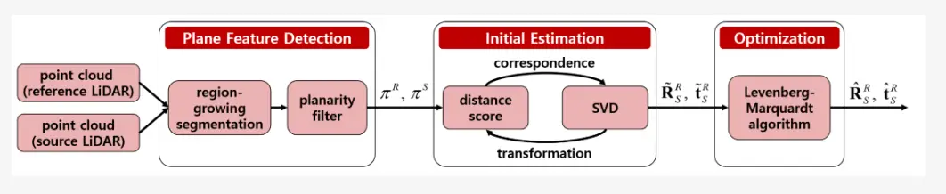
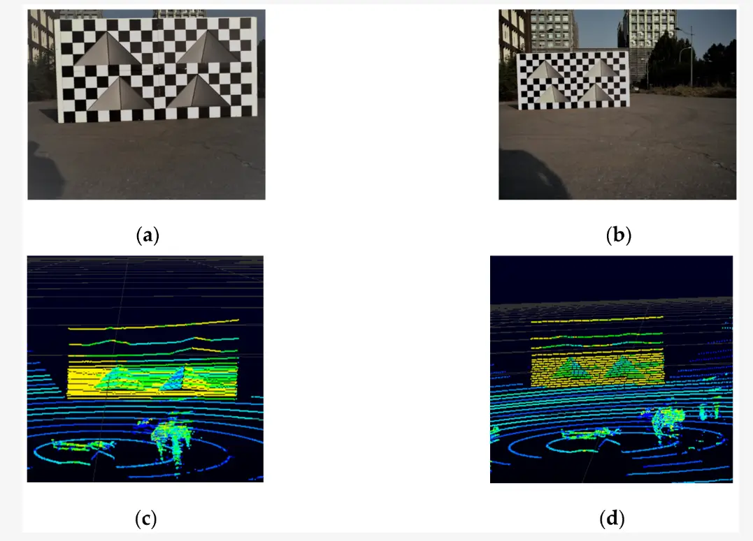
1) Extrinsic Calibration of Multiple 3D LiDAR Sensors by the Use of Planar Objects
2) Photonic Integrated Circuits for LiDAR: Solid-State 2D Beamsteering
FAQs
What are Optical Phase Arrays?
OPAs steer the beam electronically by controlling the phase of light across many emitters. There are no moving parts, making them attractive for compact and scalable designs.
What is direct and indirect Time of Flight?
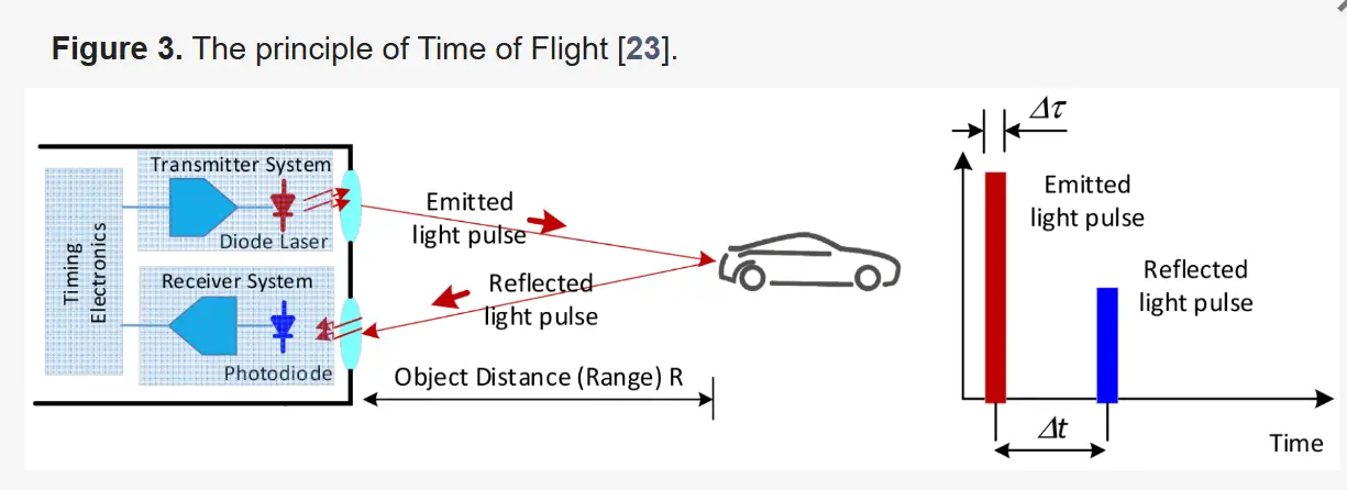
Direct Time of Flight (dToF) measures distance by sending a short laser pulse and directly timing how long it takes to return.
Indirect Time of Flight (iToF) measures distance by analyzing the phase shift of a continuous or modulated light signal rather than timing individual pulses.
What are the types of LIDAR?
The main types of LiDAR are:
- Mechanical LiDAR – uses rotating parts to scan the environment
- MEMS LiDAR – uses micro-mirrors for beam steering
- Flash LiDAR – captures the entire scene at once without scanning
- Solid-state LiDAR (OPA/FMCW-based) – uses electronic or photonic methods for beam steering with no moving parts
What is a Point Cloud?
A point cloud is a collection of data points in 3D space generated by LiDAR. Each point represents a measured position in the environment, allowing the system to reconstruct shapes, surfaces, and objects in detail.
What are LIDAR ASICs?
LIDAR ASICs (Application-Specific Integrated Circuits) are specialized, high-performance chips that integrate key electronic components of a Light Detection and Ranging system onto a single piece of silicon. By combining receivers, analog-to-digital converters, and signal processing, they enable compact, efficient, and cost-effective 3D sensing for autonomous driving and industrial robotics.


