Precision Die Targeting: Streamlined Testing and Inking
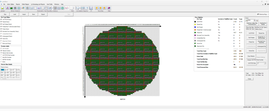
This advanced module gives users the ability to associate die with the probe site, reticle site, and WAT/PCM sites. Enables communication with Wafer prober for both test and inking functions. This Add-on module empowers users to associate die seamlessly with probe sites, reticle sites, and WAT/PCM sites. This unlocks seamless communication with your wafer prober for efficient test and inking functions.
Optimizing wafer testing efficiency and operations:
Optimizing Wafer Test Efficiency:
Ensure your wafer tests are resource-efficient by avoiding unintentionally testing the same die repeatedly. This reduces touchdowns per die, which can be critical for certain applications, such as the automotive industry, which has a limit of only 4 touchdowns per die.
Efficient Test Program Planning for Multiple Products:
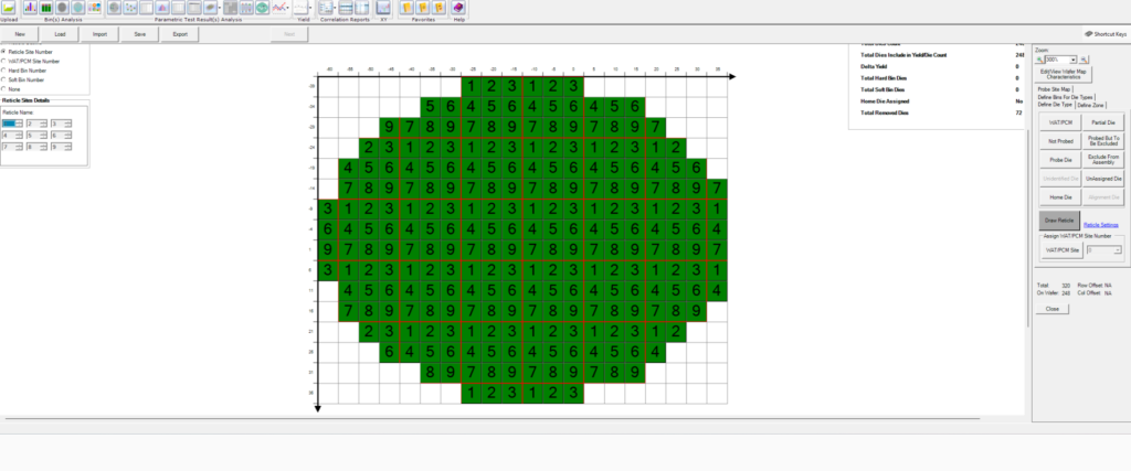
Streamline your test program planning, particularly in scenarios with multiple products on a wafer due to a 4-product mask reticle. Our module simplifies the identification and optimization of unique die touchpoints during probing, making the process less complex.
Sequencing Probing and Inking with Wafer-Level Mapping Data:
Derive your probing and inking sequence directly from wafer-level mapping data and eliminate the dependency on knowing the WAT/PCM die or partial/edge die.
Precision Die Targeting: Streamlined Testing and Inking
This advanced module gives users the ability to associate die with the probe site, reticle site, and WAT/PCM sites. Enables communication with Wafer prober for both test and inking functions. This Add-on module empowers users to associate die seamlessly with probe sites, reticle sites, and WAT/PCM sites. This unlocks seamless communication with your wafer prober for efficient test and inking functions.
Optimizing wafer testing efficiency and operations:
Optimizing Wafer Test Efficiency:
Ensure your wafer tests are resource-efficient by avoiding unintentionally testing the same die repeatedly. This reduces touchdowns per die, which can be critical for certain applications, such as the automotive industry, which has a limit of only 4 touchdowns per die.
Efficient Test Program Planning for Multiple Products:
Streamline your test program planning, particularly in scenarios with multiple products on a wafer due to a 4-product mask reticle. Our module simplifies the identification and optimization of unique die touchpoints during probing, making the process less complex.
Sequencing Probing and Inking with Wafer-Level Mapping Data:
Derive your probing and inking sequence directly from wafer-level mapping data and eliminate the dependency on knowing the WAT/PCM die or partial/edge die.