Advance Assembly Precision with yieldWerx’s Wafer Mapping Solutions
With yieldWerx, experience simplified wafer mapping and inspection in semiconductor manufacturing.
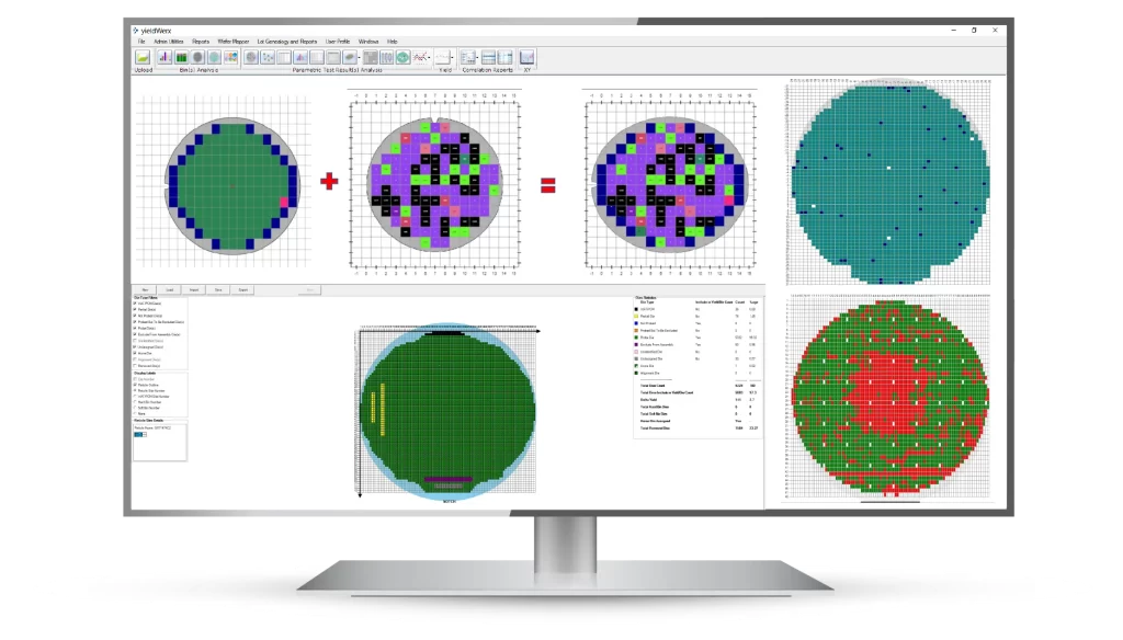
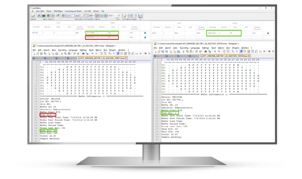
Assembly Map Generation Precision in Every Chip
yieldWerx’s Assembly Map Generation turns data into detailed maps for precise inspection and assembly, integrating with your MES for product-specific customization and equipment versatility.
Key Features of Wafer Mapping
Automated Optical Inspection (AOI) Support:
Automate optical inspection to ensure precision and quality in semiconductor wafer processing.
MES System Integration:
Connect with MES for automated assembly maps, optimizing the synchronization of wafer components.
Post-Test Analysis and Modifications:
Update wafer maps with the latest test results, improving yield through informed modifications.
New Product Introduction (NPI) Support:
Provide essential tools for new product introductions to aid engineers during development phases.
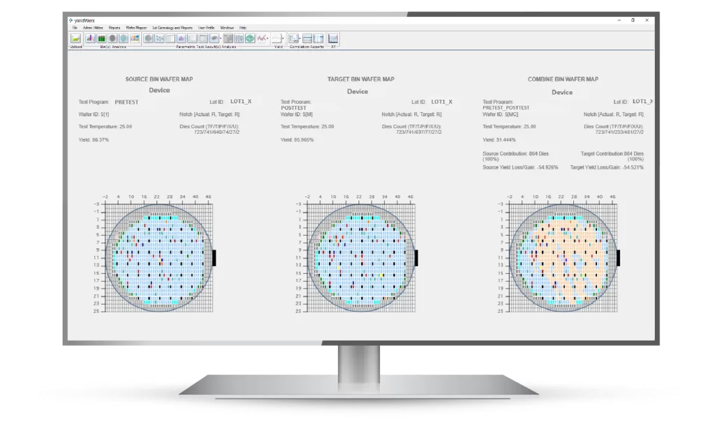
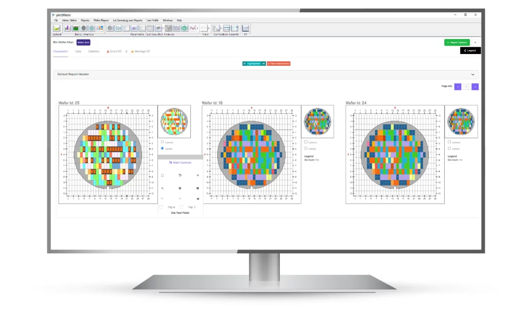
Advanced Wafer Management with yieldWerx
Support for Complex Wafer Configurations:
Manage intricate wafer structures with high-reliability needs using specialized mapping software.
Multi-OSAT Coordination:
Facilitate operations across OSATs, removing manual intervention and improving process efficiency.
Performance Binning Data Integration:
Embed performance data into maps, directing wafers to their intended packages and destinations.
Strengthen Semiconductor Processes through Adaptive Mapping and Custom Integration
Adapt Formats Flexibly:
Accommodate diverse industry formats, broadening the adaptability of your semiconductor manufacturing process.
Integrate Custom Solutions:
Incorporate custom formats, ensuring compatibility and continuous use of your existing semiconductor equipment.
Customizable Assembly Maps:
Adjust initial assembly maps based on precise AOI feedback, aligning wafer mapping with your operational efficiency objectives.
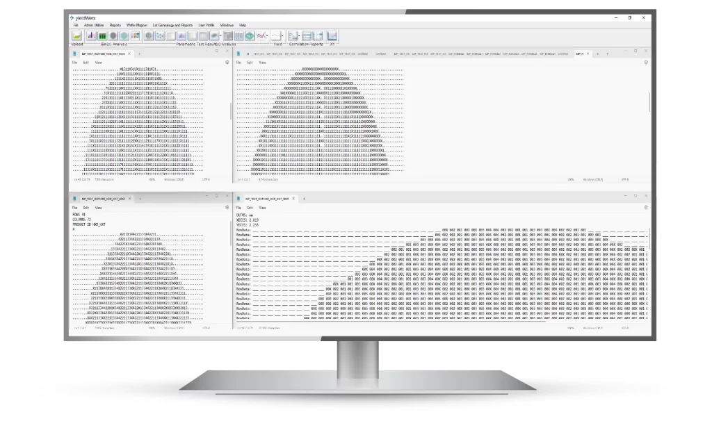

Advance Assembly Precision with yieldWerx’s Wafer Mapping Solutions
With yieldWerx, experience simplified wafer mapping and inspection in semiconductor manufacturing.

Assembly Map Generation Precision in Every Chip
YieldWerx’s Assembly Map Generation turns data into detailed maps for precise inspection and assembly, integrating with your MES for product-specific customization and equipment versatility

Key Features of Wafer Mapping
Automated Optical Inspection (AOI) Support:
Automate optical inspection to ensure precision and quality in semiconductor wafer processing.
MES System Integration:
Connect with MES for automated assembly maps, optimizing the synchronization of wafer components.
Post-Test Analysis and Modifications:
Update wafer maps with the latest test results, improving yield through informed modifications.
New Product Introduction (NPI) Support:
Provide essential tools for new product introductions to aid engineers during development phases.

Advanced Wafer Management with yieldWerx
Support for Complex Wafer Configurations:
Manage intricate wafer structures with high-reliability needs using specialized mapping software.
Multi-OSAT Coordination:
Facilitate operations across OSATs, removing manual intervention and improving process efficiency.
Performance Binning Data Integration:
Embed performance data into maps, directing wafers to their intended packages and destinations.

Strengthen Semiconductor Processes through Adaptive Mapping and Custom Integration
Adapt Formats Flexibly:
Accommodate diverse industry formats, broadening the adaptability of your semiconductor manufacturing process.
Integrate Custom Solutions:
Incorporate custom formats, ensuring compatibility and continuous use of your existing semiconductor equipment.
Customizable Assembly Maps:
Adjust initial assembly maps based on precise AOI feedback, aligning wafer mapping with your operational efficiency objectives.
Targeted Problem Resolution:
Address manufacturing challenges by seamlessly integrating data sources and employing program-specific execution strategies.
Core yieldWerx Module
The Core yieldWerx module enhances semiconductor data management with flexible yield calculations and advanced data analysis tools.

Report & Analysis
Report & analysis by yieldWerx provides data-driven decisions with comprehensive production yield reporting and in-depth analysis tools.

Quality Assurance
Quality assurance through yieldWerx ensures precision outlier detection with specialized automotive functionality.

Self-Service Capability for Report Creation
Experience flexibility and control with our self-service reporting feature, designed to suit your unique semiconductor needs.

100+ Management/SCM/Planing Widgets
Access widgets to streamline your management, supply chain, and planning activities, to optimize your operational efficiency.

Engineering & Quality Control Widgets
Use specialized widgets for engineering and design to ensure exceptional product development and stringent quality control.

Mobile Accessibility via Phone App
Stay connected with our mobile app, enabling efficient access to information and real-time alerts for semiconductor operations.
Precision in Every Chip - yieldWerx Wafer Mapping
Navigate the complexities of semiconductor assembly with yieldWerx’s Wafer Mapping Software. Our intuitive platform delivers precision mapping and AOI integration, assuring your production meets the highest standards of accuracy and efficiency. Adapt effortlessly to industry demands and drive your semiconductor processes to new heights with yieldWerx.