AI and Large Language Models (LLM) Clusters are shifting the semiconductor industry towards optical I/O on silicon photonics and co-packaged optics (CPO) which means that manufacturing data is moving from electrical only to integration with light.
Traditional semiconductor yield management relied primarily on electrical testing. Engineers measured voltage, current, leakage, timing, and signal integrity to determine whether a device was healthy.
However, a photonic integrated circuit (PIC) can pass electrical tests while simultaneously exhibiting insertion loss issues, wavelength drift, and thermal instability. These issues often remain hidden until the system-level test (SLT), at which point diagnosis becomes highly expensive.
Industry estimates suggest that defects escaping wafer-level screening and reaching final CPO assembly can cost 8x to 15x more to diagnose and remediate than defects identified during earlier manufacturing stages. This 15x penalty is becoming the strongest argument for earlier optical characterization and more sophisticated optical-electrical test data correlation.
This article will explore why electrical and optical test correlation is critical for photonics manufacturing, compare different testing approaches from wafer sort to CPO assembly, and examine the tradeoffs between test cost, coverage, and yield visibility.
We’ll also discuss what happens when electrical and optical data live in silos, and how advanced analytics can help manufacturers improve yield and reduce the cost of defect escapes.
The Data Problem Behind Photonics Scaling
Most discussions around photonics testing focus on optical alignment, instrumentation, or test coverage. Far less attention is paid to what happens after the measurements are collected.
In many manufacturing environments, electrical and optical results are generated by separate systems and stored in different formats, as there is a lack of standardization in the silicon photonics industry. Engineers may need to correlate ATE records, optical characterization data, reliability results, and assembly information to reconstruct the history of a single device. As production volumes grow from thousands of units to millions, that process becomes increasingly difficult and important.
In this scenario, electrical and optical test correlation is emerging as one of the most important capabilities for modern photonics yield management. Companies that successfully connect electrical measurements, optical characterization, reliability data, and manufacturing history will be better positioned to improve yield and accelerate root-cause analysis.
Why Electrical Testing Alone Is No Longer Enough For Silicon Photonics?
Electrical testing remains a critical component of photonics manufacturing, providing valuable insights into device health, process stability, and manufacturing quality.
The challenge is that electrical performance does not always predict optical performance. Many factors that ultimately determine product success are influenced by interactions among electrical behavior, optical characteristics, thermal conditions, packaging effects, and environmental variations.
A device may appear healthy from an electrical perspective while exhibiting optical behaviors that reduce performance or create long-term reliability concerns. These issues may not become visible until later stages of assembly or deployment, when diagnosis becomes significantly more expensive.
This is one of the fundamental differences between traditional semiconductor manufacturing and photonics manufacturing. Understanding whether a device will ultimately meet performance and reliability requirements increasingly requires visibility across multiple domains rather than a single set of measurements.
The Tradeoff Between Cost and Visibility
Every additional test operation increases manufacturing cost and cycle time. Yet insufficient testing increases the risk of defect escapes reaching expensive downstream assembly stages.
This balance between cost and visibility has become one of the defining challenges in advanced photonics manufacturing.The table highlights a challenge every photonics manufacturer faces.
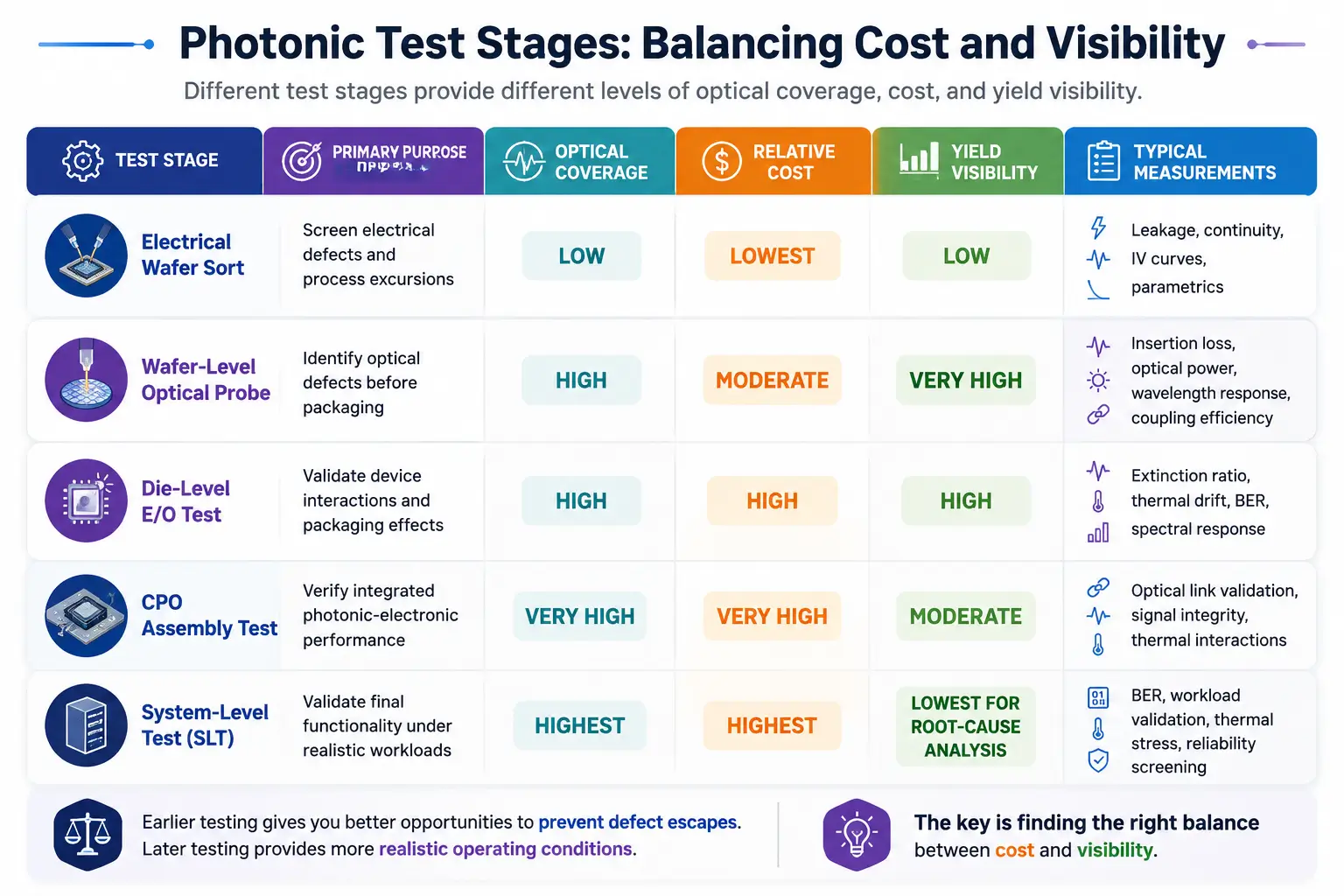
Earlier testing provides better opportunities to prevent defect escapes. Later testing provides more realistic operating conditions. The difficulty lies in finding the right balance.
This is why wafer-level optical probing is becoming increasingly important across the industry. Manufacturers want to identify optical defects before expensive packaging and assembly operations add significant value to the device.
The 8–15X Cost of Defect Escapes in Co-Packaged Optics
The economics become even more compelling in CPO environments.
Industry estimates suggest that defects escaping wafer-level screening and reaching CPO assembly can cost 8–15X more to diagnose than defects identified during earlier manufacturing stages.
The reason is straightforward.
A wafer-level optical defect typically involves a single die and a relatively small amount of engineering investigation. The same issue discovered at later stages may require investigation across multiple interacting subsystems.
At the CPO level, failures can originate from photonic devices, lasers, optical interfaces, packaging interactions, thermal effects, or neighboring electronic components. Determining the root cause often becomes a multidisciplinary exercise involving design, test, packaging, reliability, and manufacturing teams.
For many organizations, this is becoming the strongest argument for earlier optical characterization and more sophisticated optical test data analysis.
Why Optical Testing Alters the Yield Equation
Unlike traditional semiconductor testing, where electrical signals can be measured through direct contact with device pads, optical characterization requires interacting with light. That seemingly simple difference introduces an entirely new layer of complexity. Light must be coupled into and out of microscopic photonic structures with extreme precision, often requiring alignment tolerances measured in fractions of a micron.
Small variations in alignment, temperature, wavelength, or polarization can influence results. In some cases, test systems must actively adjust multiple variables simultaneously to achieve stable and repeatable measurements. What is a relatively straightforward electrical measurement can become a far more intricate optical characterization process.
This complexity has a direct impact on manufacturing. Optical testing typically takes longer, requires more specialized equipment, and adds cost compared to traditional electrical testing. Yet for many photonic devices, it is the only way to gain visibility into the characteristics that ultimately determine performance, reliability, and yield.
The result is a constant balancing act. Manufacturers want earlier optical visibility to prevent costly defect escapes, but they must also manage throughput and cost-of-test targets. This makes every optical measurement increasingly valuable.
In high-volume photonics manufacturing, the goal is not just to collect optical data. It is to extract as much intelligence as possible from every measurement and connect those insights to the broader manufacturing process.
Thermal Drift: A Perfect Example of Why E/O Correlation Matters
One of the biggest challenges in photonics manufacturing is that electrical and optical performance do not always move together.
A device can appear healthy from an electrical perspective while experiencing optical behavior that impacts performance or long-term reliability. Thermal drift is a common example. As temperatures change, photonic structures can experience shifts in wavelength and optical response, potentially increasing insertion loss or reducing signal quality even when electrical parameters remain within specification.
Viewed in isolation, neither the electrical data nor the optical data tells the full story. Electrical measurements may show no indication of a problem, while optical measurements alone may reveal an issue without explaining its underlying cause.
What Happens When Electrical and Optical Data Live in Silos?
Modern photonics manufacturing produces information at every stage of the lifecycle, from wafer-level characterization and optical probing to assembly, reliability qualification, and system-level test (SLT). Yet these datasets often reside in different systems, owned by different teams, and analyzed in isolation. The result is limited visibility into how devices behave as they move through manufacturing.
A yield issue identified during SLT may have originated from a wafer-level process variation. An optical performance problem observed after packaging may be linked to an earlier electrical signature. A reliability concern discovered in the field may trace back to manufacturing conditions that were visible months earlier but never connected to downstream results.
When data remains fragmented, those relationships are difficult to identify.
Manufacturers lose the ability to understand how electrical behavior influences optical performance, how wafer-level signatures relate to final product quality, and which process variations are driving yield loss across the manufacturing flow. Root-cause analysis becomes slower, yield learning cycles lengthen, and defect escapes become more difficult to prevent.
Real-World Examples of Electrical and Optical Test Correlation
Example 1:
During wafer-level and chip-level testing, engineers routinely correlate alignment position data with optical power and insertion loss measurements. Small alignment variations can significantly impact coupling efficiency, making alignment-to-loss correlation a critical part of photonics testing and yield optimization.
Example 2:
In silicon photonics manufacturing, engineers increasingly correlate wafer-level opto-electrical test data with downstream optical measurements to identify process variations that impact final device performance. This enables earlier defect detection and improves yield learning before costly packaging and assembly operations.
Can Photonics Borrow the Semiconductor Yield Playbook?
For anyone coming from traditional semiconductor manufacturing, many of these challenges sound familiar.
- Wafer defect correlation.
- Yield learning.
- Process excursion detection.
- Traceability.
- Root-cause analysis.
The semiconductor industry has spent decades building methodologies to solve these problems.
Photonics does not need to reinvent that playbook, it needs to extend it.
The difference is that semiconductor engineers primarily analyze electrical parameters, while photonics organizations must correlate electrical, optical, thermal, packaging, and reliability data simultaneously.
The organizations that successfully adapt semiconductor yield methodologies to optical datasets will gain significant advantages in photonics yield management and silicon photonics analytics.
The Rise of PIC Yield Analytics, Chiplet Data Analytics, and CPO Analytics
As photonics manufacturing matures, analytics is becoming a competitive differentiator.
Modern PIC yield analytics platforms combine electrical measurements, optical characterization, wafer maps, assembly history, reliability data, and SLT outcomes into a unified analytical environment.
This enables engineers to perform wafer defect correlation across multiple manufacturing stages.
A yield excursion discovered during system-level testing can be traced back to wafer-level optical measurements. Reliability failures can be linked to process signatures observed months earlier. Optical degradation can be connected to specific fabrication conditions, packaging variables, or assembly operations.
The same trend is driving growing demand for chiplet and CPO data analytics as manufacturers seek visibility across increasingly complex heterogeneous systems.
The objective is no longer simply finding failures. It is understanding why they occur.
Looking Ahead
The rapid growth of AI infrastructure is accelerating the adoption of silicon photonics, optical chiplets, and co-packaged optics. But as bandwidth requirements increase, so does manufacturing complexity.
The industry’s next challenge is not just building faster photonic devices but also building the visibility required to manufacture them at scale.
Electrical testing alone can no longer provide that visibility. Optical testing alone cannot provide it either.
The future of photonics yield management lies in connecting electrical measurements, optical characterization, thermal behavior, reliability data, assembly history, wafer maps, and SLT outcomes into a unified view of manufacturing performance.
Because in advanced photonics, the most valuable insight is rarely found in a single test result.
It emerges when all of the data is integrated.
Ayar Labs put this into practice. According to their CIO, Garth Thompson, collaborating with yieldWerx gave them “measurable results in just 30 days” by integrating their complex photonics data to accelerate yield and quality decisions.
Yield Analytics, built for Advanced Photonics. Contact yieldWerx for a free consultation.
References:
1) SemiEngineering: Co-Packaged Optics Testing Faces Steep Data Center Ramp
2) Silicon Photonics for AI – Balancing Cost, Power, and Reliability
3) Testing At The Speed Of Light: Enabling Scalable Optical Testing For Silicon Photonics And CPO
4) Challenges In Testing Photonics In Chips
FAQs?
How is Electrical and Optical Test Data Correlated?
Electrical and optical test data are typically correlated by assigning each die or package a unique identifier—such as a wafer ID, die coordinates, serial number, or barcode—and using that identifier to merge results from different test stages. Analytics platforms then combine electrical ATE data, optical measurements, assembly records, and SLT results into a single device history, allowing engineers to trace failures and identify patterns across the manufacturing flow.
What is Wavelength Drift in Silicon Photonics?
Wavelength drift is the shift in the operating wavelength of a photonic device due to changes in temperature, voltage, or environmental conditions. In devices such as micro-ring modulators, even small wavelength shifts can increase insertion loss and reduce overall optical performance.
What is Optical Coupling?
Optical coupling is the process of transferring light from one optical component to another, such as from an optical fiber into a photonic integrated circuit (PIC). Efficient optical coupling minimizes signal loss and is critical for achieving high-performance photonic systems.
What is Thermal Drift in Silicon Photonics?
Thermal drift refers to changes in the optical characteristics of a photonic device caused by temperature fluctuations. As temperatures change, properties such as refractive index and resonant wavelength can shift, affecting performance and requiring compensation or calibration.
What is Optical Alignment?
Optical alignment is the process of precisely positioning optical components—such as fibers, lasers, or waveguides so that light can be transferred between them with minimal loss.
What is Defect Escape?
A defect escape occurs when a faulty device passes one stage of testing undetected and progresses to a later manufacturing stage or reaches the customer. In advanced photonics and co-packaged optics, defect escapes become increasingly expensive because they are often discovered only after high-value packaging and assembly processes.
What is Wafer-Level Testing?
Wafer-level testing is the process of evaluating semiconductor or photonic devices while they are still part of the wafer, before they are cut into individual dies. Early testing helps identify defective devices sooner, reducing packaging costs and improving overall manufacturing yield.
What is System-Level Testing?
System-Level Testing (SLT) is the final stage of manufacturing validation, where a fully assembled device or module is tested under conditions that closely resemble real-world operation. In photonics, SLT verifies that integrated electrical and optical components function correctly together before shipment.