Semiconductor Manufacturing is not a stranger to “Big Data”. Intel alone manages 59 Data Centers and over 130,000 servers for its internal design and manufacturing operations. In fact, the capital equipment cost for a new Flash memory or Logic fab in 2016 is estimated to be at least $6-8B with each fab supported by a large dedicated data center.
Semiconductors generate big data in 3 places: Design, Wafer Manufacturing and Device Testing. Design data culminates in files to generate up to 100 photo masks and can take thousands of CPU’s a week or more to “Tape Out” these files. Wafer fabs collect lots of machine and metrology measurements in a discrete manufacturing environment. Finally, 100’s of devices on a wafer are tested, packaged and tested again to become the final product.
The term real-time differs dramatically for the 3 data spaces because of the different throughputs. Real-time isn’t relevant to design data (fast analysis and synthesis is important but designs take months and years). Wafer manufacturing uses cassette carriers so real-time means tracking the metrics associated with movement of the wafers in these cassettes (milliseconds to hours to work weeks). Finally, device testing programs can run the chips at high speeds (nanoseconds or faster) to make pass-fail decisions, but inter-die decisions usually take seconds and inter-wafer analysis minutes or hours.
AMD claims that it has accomplished nearly 90 percent production yields in manufacturing of its Opteron processors by minimizing – faulty devices by capturing and analyzing terabytes of wafer data in near real-time. Likewise, Samsung is running data analytics on up to 80 terabytes of data in its fab in Hwasung to ensure energy efficiency in its chips.
Semiconductor fabs— one of the most heavily instrumented manufacturing facilities in today’s industrial landscape— continue to grow their data infrastructure in order to improve yield and equipment throughput (up to 80% of cost is equipment depreciation) without compromising quality. The amount of data in semiconductor manufacturing is rising exponentially with the increase in design complexity amid larger memories, system-on-chip (SoC) and multi-core designs and the fact that leading edge manufacturing processes are moving toward 20 nm and below. The life cycle of a chip generates petabytes of data, although much of it is discarded after a pass/fail decision or not retained after wafers and devices are shipped.
Because chip manufacturing operations produce tons of data, one of the challenges in utilizing the big data environment is to analyze across operations (often multiple vendors), extract systematic signals from noise and generate actionable insights in “real-time”.
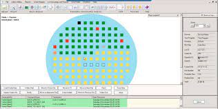
One example is the company QuickLogic who is the maker of ultra-low-power chips for smartphones, wearables and the Internet of Things (IoT) devices. The Sunnyvale, California–based chip maker is now using yieldWerx Enterprise to formulate data analysis reports in real-time and send them to wafer fabs and test houses for quick team-based decision making. That allows QuickLogic, and their partner’s engineers, to analyze the defect root cause types of yield loss and save up to 90 percent of the time previously spent in manually extracting and cleansing the data.
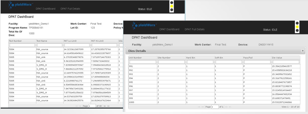
yieldWerx Enterprise allows QuickLogic to perform early defect detection
yieldWerx Enterprise is a data warehousing, root cause analysis and automated monitoring and reporting tool that allows chip makers, like QuickLogic, to carry out data extraction, transformations and loading product and lot genealogy data from ATE and MES systems. It enables QuickLogic’s engineers to efficiently find and correct systematic operational issues that impact yield and quality, which in turn, leads to faster production ramps, higher yields and lower manufacturing costs.
Moreover, they don’t have to maintain and run their batch analysis jobs and are more productive and efficient with their time. The actionable information available from yieldWerx Enterprise is available to other teams like quality and manufacturing operations to allow them to pinpoint fabrication errors and processing inefficiencies in near real-time.
Semiconductor manufacturing operations already boast sophisticated engineering data analysis that includes heaps of data sets. However, what the big data revolution brings to the table is a shift from human-driven to more automation in data collection, quality monitoring and exception handling of these operations in a globally outsourced supply chain.
Find out more about how yieldWerx is helping QuickLogic to boost engineering productivity.