Processing the big data from sensors or test equipments in a production line is a powerful strategy to big data analytics in real time the health of your products. It gives a clear advantage to your company in fixing problems faster and thus improving the productivity of the assembly line. The amount of data to track possible failures is increasing every year since the demand of better quality and production volumes are growing. Indeed, in the semiconductor sector, since the late 2000’s the volume of data has been multiplied by 7 in 10 years, reaching in 2019 around 40 000 trillion of data points, with a significant increase in the etch and deposition processes.
However, many companies still need to switch to better production management systems since in average only 0.5 % of the data is used for making important decisions. This means that both useful and colossal volumes of data remain unexploited. Being in possession of powerful analytic tools will give a competitive advantage to your Fab, by releasing the potential of these huge amounts of data some possible improvement options will be more likely to emerge.
At yieldWerx, we provide an efficient management interface designed for the entire supply chain, our clients rely on us to monitor billions of chips annually. The traditional analysis is based on first gathering the data, getting information, proposing an observation and finally making decisions. However, the advanced analytics solution we propose start from the human stage where depending on what decisions needs to be made, proposed insights, information and data will be given. Our powerful big data analytic modules can help you in many ways not to only improve your mature products but also ramp up in an average 10 % faster the new technologies:
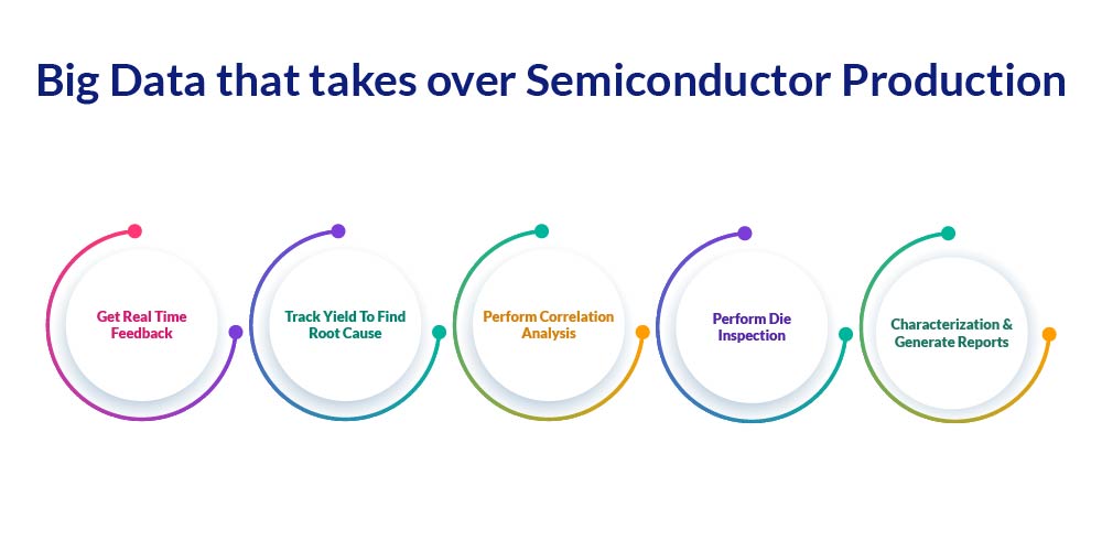
- Get in-real-time feedbacks by e-mail from our SPC module when an anomaly of a monitored parameter is detected, use the software to hold the possible lots at risk. You can then decide whether a maintenance on the equipment is necessary or not.
- Follow each wafer through the complete process steps by visualising the Lot Genealogy from ATE and MES systems. Track the yield across the production line to highlight more easily the root cause of productivity decrease.
- Perform correlation analysis between work centers and the final test to detect early yield reduction factors. Use this information to straighten up again the yield and the profits of your Fab.
- Perform die inspection with Smart Probe, convert the data in many formats and use it to generate bin histograms. The wafer maps are interactive: it allows zonal selection and displays the yield and other information for the selected area.
- Your data is sorted on the same interface by facility, work center, device name, test program, lot, wafer and parameters, making it easy to access. Many report options can then be selected to generate clean processed data.
- Are you stepping into the automotive market? In one of our blogs, we present you the PAT and GDBN analytics modules adapted to these specific products. yieldWerx indeed provides these statistical screening methods to respect the AEC (Automotive Electronics Council) Q002 guideline for statistical yield analysis.
- Characterize and generate reports associated with new technologies. Reduce the ramping process by adjusting faster the key parameters and yield engineering criteria.
Whether you represent an international semiconductor group or an IC startup, yieldWerx Enterprise can be fully customized and adapted to treat your big data analytics. You will save precious time on ramping-up new technologies with efficient characterizations and improving the yield of mature dies by using much more data than traditional methods to spot out the root causes faster. Take a 15 days free trial or schedule a demo to uncover the potential of your data when processed by yieldWerx Enterprise.


