
End-to-end Semiconductor Data Analytics and Traceability Solutions For Multi-Chip Packages
Efficient test data integration is crucial for producing reliable multi-chip packages (MCPs. However, fabless companies, IDMs and OSATs face significant challenges in handling diverse test data formats associated with individual chips forming any package. Traditional approaches, such as manual checks and correlating individual logs, are no longer sufficient to meet the demands of modern chip production having a global supply chain footprint.
Enter the yieldWerx Genealogy module—a powerful solution designed to transform test data analysis and integration for MCPs. When coupled with custom data parsers designed by our in-house team of experts, it links defect data across multiple stages and devices enabling companies to optimize their yield management efforts. The top benefits are early defect detection and correction, increased reliability, shorter time-to-market and eventually increased profitability.
In this blog post, we’ll discuss:
- What are MCPs?
- How do semiconductor companies struggle with test data management?
- Why test data traceability is crucial for yield enhancement?
- How yieldWerx helps you deal with these challenges?
Want to See Things In Action? Schedule a Demo Today
What are Multi-Chip Packages (MCPs) and Its Types?
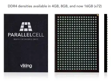
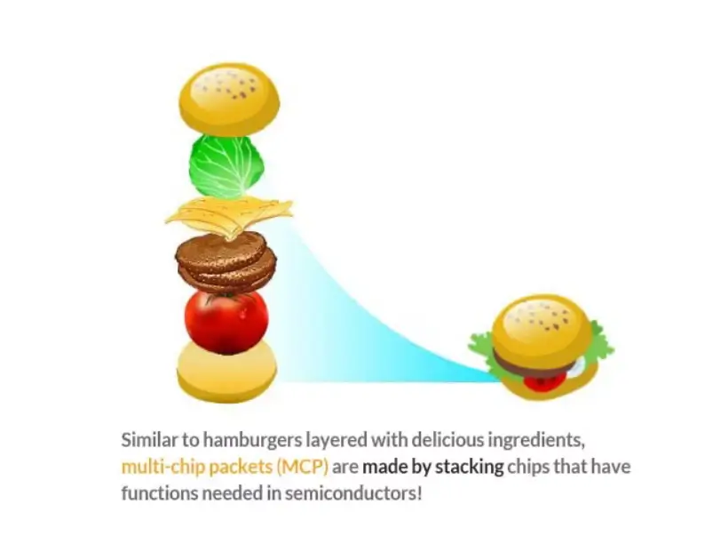
MCP, or Multi-Chip Package, refers to a technology that combines two or more semiconductor chips into a single package. While it appears as one semiconductor from the outside, it actually contains multiple chips inside. Unlike arranging individual semiconductors horizontally, MCPs stack chips vertically, significantly reducing the space they occupy, making them essential for compact devices like smartphones, tablets, and other portable electronics. Samsung uses the analogy of stacking a burger. Bun, cheese slice, patty, vegetables and other fillings make up a burger. Similarly, different chips are the ingredients that form an MCP. Each one can come from a different source.
System-in-Package is a similar concept. Instead of mounting chips on a printed circuit board, they can be integrated into a single package to reduce costs and minimize the distance electrical signals need to travel.
Then, there is the good old IC PCB board with integrated circuits (ICs) mounted on the board. Typically, you solder an IC to the surface of the PCB assembly and the wires attached to it.
How Do Semiconductor Companies Struggle With Test Data Management?
In semiconductor manufacturing, chips go through several testing stages. All these stages produce enormous amounts of data. Moreover, varying types of chips face varying testing systems. For example, memory and power chip test systems are different and may produce data outputs in completely different and even proprietary formats.
As MCPs are made of multiple chips, it is important to have a consolidated test dataset for complete insights. Overall, there is a lack of standardisation in the test data analytics industry and companies often end up going through manual data checking.
Some commonly used data formats are STDF, ATDF, CSV, JSON, XML, LOG, and DAT. This number can easily cross 100 but STDF remains the gold standard.
Traceability is Crucial for Yield Enhancement
Semiconductor companies actively rely on data from WAT, Wafer Sort (WS), and Final Test (FT) to uncover defects, but when problems arise during any of these phases, tracing the root cause is critical. Engineers must determine whether the issue is isolated to a specific wafer or impacts all wafers from a particular production run. This requires a robust traceability system capable of correlating every test ever conducted on every chip, enabled by an embedded chip ID (ECID).
The ability to quickly receive and analyze test data from all manufacturing test stages, while simultaneously cross-correlating that data to identify trends and implement corrective actions is crucial for semiconductor yield enhancement.
Building on the burger analogy, in a top-tier burger joint, every ingredient has sourcing details like
where and when the patty was made, when the cheese was sliced, and how fresh the vegetables were.
What happens if too many customers complain about the food quality in a short period?
Food managers begin with standard quality checks. They review the freshness of every ingredient, their sourcing details, recipe and even CCTV footage. This way they can quickly isolate issues like mouldy ingredients, cooking time errors or a combination of reasons. Later, they can refine processes to ensure every ‘burger’ (MCP) meets the highest quality standards and that customers keep returning with positive reviews (no RMAs).
yieldWerx Turning Test Data into Actionable Insights
To address these challenges, yieldWerx team has developed multiple parsers capable of handling diverse test datasets rapidly. These parsers enable yield engineers, test engineers, and product managers to extract specific information for root-cause analysis while dealing with various system-in-package (SiP) or IC board data.
The Lot Genealogy module acts as the core of the solution that integrates diverse and huge datasets providing a unified view of MCP yield analysis. This includes analyzing the multi-chip package from the level of individual devices, allowing early test and inspection screening.
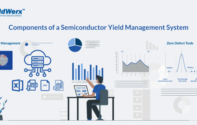
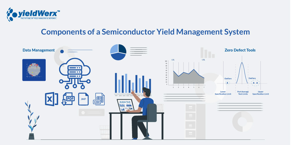
Our yield management system offers straightforward and customizable analysis options for your specific needs and includes tools to create detailed visualizations for better decision-making. It has all the charting and reporting tools a semiconductor test engineer would expect.
Engineers can identify upstream parameters that predict downstream failures, such as chips failing at the final test (FT). Detecting these issues earlier during WAT or WS test phases leads to significant cost savings and increased productivity.
Unrecognized or Unsupported Map Formats?
If you encounter a map format that you cannot convert or identify, please send us a sample or two at info@yieldwerx.com
Providing additional details, such as the file’s source, can help us locate relevant documentation. We’ll gladly review the format to determine if it aligns with an existing format we support or if a suitable alternative is available.
FAQs:
What is a Data Parsing?
It means extracting and organizing raw test data into a structured format for analysis.
What is WAT?
Wafer Acceptance Test (WAT) checks electrical parameters on test structures after wafer fabrication.
What is Wafer Sort?
A test phase that screens individual dies on a wafer before packaging to identify defects.
What is a Final Test?
The last test stage ensuring packaged chips meet performance and quality standards before shipment.
What is ECID?
Embedded Chip ID (ECID) is a unique identifier for each chip, enabling traceability across manufacturing stages.

