In the semiconductor manufacturing industry, yield management systems play a crucial role in maximizing productivity and profitability. By tracking and analyzing the data generated during the manufacturing process, these systems can identify and rectify issues that impact yield, ultimately resulting in better product quality and increased profits. However, with so many options available, it can be challenging to determine what features are essential for an effective yield management solution.
In this writeup, we will discuss the key components that manufacturers should look for when choosing a semiconductor yield management system.
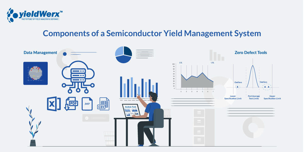
1.Data Management:
Data management is a crucial component of any yield management system. The system should be able to handle large amounts of data collected from multiple sources, including wafer fabs and OSATs. It should also define the genealogy between data sources, making it easier to track issues and determine their root causes. The system should be able to quickly access the data and automate data parsers to process multiple data formats without the need for further development.
2.Analysis Tools:
The following analysis tools are essential for any yield optimization system:
1. Yield Analysis:
Yield analysis is a crucial tool for identifying yield issues that impact yield. By analyzing the yield data, the system can identify trends and patterns that may indicate an issue in the manufacturing process.
2. Wafer Map Analysis:
Wafer map analysis is another essential tool that helps manufacturers track the performance of each wafer in the manufacturing process. By identifying wafer defects, the system can pinpoint the root cause and corrective actions implemented to improve yield.
3. Parametric Analysis:
Parametric analysis measures the electrical properties of each device and compares them to the desired specifications. This analysis helps manufacturers identify any deviation from the desired performance and correct them in real-time.
4. Bin Analysis:
Bin analysis is used to group devices with similar characteristics together. This analysis is used to identify defects that are impacting yield.
5. WAT/PCM:
Wafer Acceptance Test (WAT) and Process Control Monitor (PCM) testing are essential tools that help manufacturers verify the performance of each device earlier in the process. This analysis helps identify issues that may impact yield and allows for real-time corrective action.
6. Excursion Analysis:
Excursion analysis helps manufacturers identify any deviation from the standard manufacturing process. By analyzing the data generated during these deviations, manufacturers can identify the root cause of the excursion and corrects them to improve yield.
7. Correlation Analysis:
Correlation analysis is used to determine the relationship between different variables and their impact on yield. This analysis helps manufacturers identify the variables that are most critical to yield and monitor them more closely.
8. Pattern Detection:
Pattern detection is used to identify any recurring issues in the manufacturing process. This analysis helps manufacturers identify the root cause of these issues and take corrective action.
9. Drift Analysis:
Drift analysis is used to identify any long-term changes in the manufacturing process that may impact yield. By identifying these changes, manufacturers can recalibrate the process to shift it to the desired target and improve yield.
10. Gage R&R:
This is used to measure the repeatability and reproducibility of the manufacturing process. This analysis helps manufacturers identify any issues with the measurement system and apply improvements to ensure consistencies particularly in electrical test.
11. Calculated Tests/Multivariate Analysis:
Calculated tests and multivariate analysis are used to analyze multiple variables and their relationship to yield. This analysis helps manufacturers identify the most critical variables that affects device performance and yield.
3. Zero Defect Tools:
In addition to the analysis tools mentioned above, an effective system for yield management it should also include zero defect tools that help manufacturers identify and eliminate potential defective parts in the manufacturing process.
The following tools are essential for achieving zero defects:
1. PAT (Part Average Test):
One of the most common tools is Part Average Test (PAT), which assesses the quality of parts by analyzing their performance against the normal distribution. This test can be run both statically and dynamically. Static PAT measures the average performance of each device, while dynamic PAT has the advantage of measuring the performance over time and is therefore mostly being the preferred option.
2. Multi-Variate PAT (MVPAT):
MVPAT is another tool used to identify outliers. It involves running multiple parameters and analyzing their relationships to define and detect outliers, which could indicate a defect.
3. Good Die Bad Neighborhood (GDBN) and Good Die Bad Neighborhood Z (GDBNZ):
GDBN and GDBN-Z are spatial analysis tools that can identify outliers by comparing the performance of a part to the performance of neighboring parts.
In conclusion, semiconductor yield management systems are critical for modern chip manufacturing. When selecting a yield optimization system, it is important to consider the data management capabilities, analysis tools, and zero-defect tools. Each tool provides critical data insights, and together they ensure optimal productivity, maintain high-quality standards, and prevent wastage.
To learn more about how “yieldWerx” YMS can enhance production yield, decrease test time, and accelerate product launch, take step for a 15 day free trial and Schedule a Live Demo.