
What do Google search, Facebook’s recommendations and modern wafer defect detection have in common?
They all rely on knowledge graphs (KGs) to process intricately complex, interlinked data.
What are Knowledge Graphs?
Knowledge graphs organize data from different sources with varying structures. They create the clearest view of defect traceability by connecting nodes, edges, and labels.
In the case of Google, KGs store data for search and retrieval tasks to provide users with a seamless research experience. This process, called semantic enrichment, allows the graph to understand individual objects and their relationships.
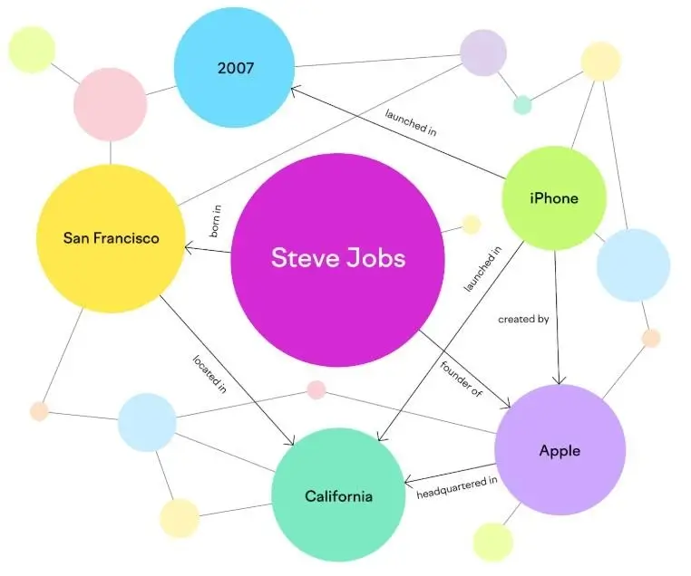
Google’s Assumed Knowledge Graph for Apple Inc. Source: SEMRush
The same methodology can be applied to semiconductor quality control. Considering the challenges posed by process precision reaching sub-5 nm levels, it becomes difficult for traditional quality inspection methods to catch up with the sheer volume and complexity of data generated.
In this guide, we’ll explore how KGs and a popular deep-learning technique called Convolutional Neural Networks (CNNs) are at the core of modern wafer defect detection, enabling manufacturers to meet the increasingly stringent demands of modern chip production.
In the end, we’ll discuss how yieldWerx’s Defect Management Module can help optimize semiconductor yield, reducing material waste and improving product reliability.
Why Traditional Manual Inspection Fall Short?
Imagine trying to find a needle in a haystack, but the haystack keeps growing and the needles keep changing shape.
This is similar to the challenge test engineers face in semiconductor manufacturing today, where defects are constantly evolving and the scale of production continues to increase. On average, a semiconductor wafer undergoes between 500 to 1,000 steps before completion.
Here’s why manual inspection and traditional image processing methods fall short for wafer surface defect detection.
Limitations of Manual Inspection
Manual inspection is still widely used in the semiconductor industry but it doesn’t detect localized failure patterns. Inspectors struggle with both efficiency and accuracy, making it difficult to meet the high precision standards. The quality of inspection can vary due to differences in judgment regarding what is considered good or bad. Inspectors’ varying skill levels can influence their assessments, leading to inconsistencies.
Challenges of Large-Scale Production
As wafer production scales up, manual inspection becomes less effective. New production defects may arise continuously, often without labeled data to identify them. Even when known defect patterns exist, labeling them is time-consuming, costly, and requires expert knowledge.
Inadequacy of Traditional Image Processing Techniques
Traditional image signal processing techniques have been commonly used in wafer surface defect detection. While these methods have their place, they often fall short when faced with the dynamic and intricate nature of semiconductor defects. Common techniques include wavelet transform, spatial filtering, and template matching.
Spatial filtering
Spatial filtering is an established image enhancement technique used for image denoising by applying spatial convolution to gray values without causing blurring. It employs smoothing and sharpening filters to improve image quality, which is particularly useful for defect detection. Methods like median and mean filters are commonly applied to reduce noise.
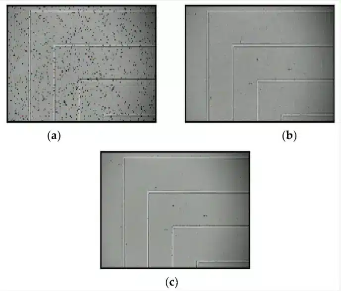
(a) original image, (b) median filter denoising, and (c) mean filter denoising.
However, the effectiveness of spatial filters is heavily dependent on selecting the right internal parameters, which can be challenging. The technique may blur fine details, making small manufacturing defects harder to detect.
Efficient image compression and local storage options are critical for post-processing and data management, especially since some defects are detectable at a very granular level (single pixel). The resolution requirements also increase the file size of images, which complicates post-processing.
yieldWerx offers a comprehensive suite of solutions for both suppliers and consumers of automotive parts. Contact Us and learn how you can achieve Zero PPM manufacturing goals.
Common Wafer Surface Defect Patterns
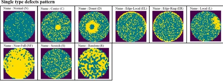
Source: Engineering Application of AI Journal Paper
Line Defects
These appear as continuous lines on the wafer, often caused by issues during the lithography or etching process. They can result from scratches, contamination, or equipment malfunctions and may affect the functionality of semiconductor devices if they cross critical paths.
Center Defects
Located at the center of the wafer, these defects typically result from issues with the wafer processing or handling, such as contamination or uneven deposition. They can affect the entire device’s performance if in critical areas.
Donut Defects
Ring-shaped defects that typically form around the center or along the edges of the wafer. They are often caused by uneven material deposition or etching, creating a circular ring of defective areas.
Scratch Defects
Linear or curved marks on the wafer’s surface caused by mechanical damage or contamination during handling, transport, or cleaning. These defects can cause failure points, particularly if located in sensitive areas.
Moon Defects
Moon-shaped defects are typically crescent-shaped and usually occur due to variations in the deposition process control. These defects can be caused by shadowing effects, contamination, or issues with the mask alignment.
Reticle Defects
Reticle defects are related to the photomask/reticle used in the lithography process. Any defects on the reticle, such as particles or imperfections, can result in corresponding defects on the wafer during the photolithography step, leading to patterning issues like missing or distorted features.
Edge Defects
These defects appear along the edges of the wafer and are often caused by handling, contamination, or mechanical stresses during processing.
It is important to know that test engineers frequently encounter combinations of these defects and must address them accordingly.
Wafer Defect Detection Complications in Complex Stacked Chips
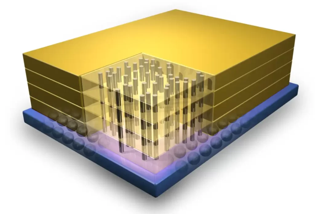
Stack of individual chips connected by ‘through silicon vias’ (TSVs). Credit: IBM
Modern stacked chip architecture offers several benefits such as reduced power consumption and space requirements. However, they pose several challenges with regards to defect detection. Here we discuss some of them.
Defect Identification in Stacked Layers:
With the multi-layered structure of stacked chips, defects in one layer can be difficult to detect because they may be hidden beneath other layers. For instance, defects such as voids in the glue or cracks in the silicon substrate, which may not be visible from the surface, need advanced imaging techniques like Near-Infrared (NIR) microscopy for detection.
Small Features and High Aspect Ratios:
The formation of Through-Silicon Vias (TSVs) with small diameters (as small as 5 µm) and high aspect ratios poses a challenge for traditional metrology tools. Accurate measurement of such small and complex features requires high-resolution optical systems that can penetrate through stacked layers without compromising resolution.
Wafer Thinning and Back-Side Processing:
After wafer thinning, there is a need for precise measurements of the remaining silicon thickness (RST) below TSVs. The process of thinning and back-side processing creates rough surfaces and introduces new potential defects, requiring specialized techniques to measure and detect these changes accurately.
Co-Planarity and Gap Measurement:
During die stacking and bonding, ensuring the uniformity of pillar height and co-planarity becomes crucial. The challenges in detecting gaps or misalignment between stacked layers can affect the overall reliability of the final device. Gaps that vary across the wafer, especially at the edges, are often harder to detect and need advanced measurement methods.
Quality Control Variations Due to Dispersed Supply Chain
Semiconductor supply chain is spread throughout the world. Any variation in quality control systems across different regions can lead to inconsistencies in the quality of materials or components used at different stages of production. This complicates defect detection, especially in cases where defects may emerge only after certain stages in the production process. Data traceability becomes highly crucial for yield management. Organizations like NIST and SEMI have developed several quality control and transportation standards to mitigate this issue.
Supercharging Wafer Defect Detection Using Knowledge Graphs and Convolutional Neural Networks
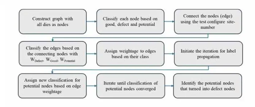
Source: Overview of the proposed graph-based semi-supervised learning methodology
Combining CNNs and KGs for wafer defect detection presents a powerful approach in semiconductor manufacturing, where both image-level accuracy and process-level understanding of failure modes and effects are essential.
What are Convolutional Neural Networks?
CNNs serve as highly capable visual analyzers, trained to process optical or SEM (Scanning Electron Microscope) images of wafers and detect a range of defects, including scratches, donut-shaped patterns, edge anomalies, contaminants, and electrical issues like opens and shorts. These supervised learning networks output feature maps, predict defect types, and calculate confidence scores—essentially acting as intelligent microscopes that not only see but also classify what’s on the wafer.
Traditional machine learning methods like decision trees, random forests, or support vector machines (SVMs) typically require manual feature extraction, where someone must carefully design features (like edges, shapes, or textures) to represent the data well.
CNNs automatically learn hierarchical features directly from raw data (such as pixel values). They are well-suited for image data because they can extract low-level features (edges, textures) in the first layers and complex high-level features (objects, patterns) in deeper layers. This eliminates the need for manual feature engineering.
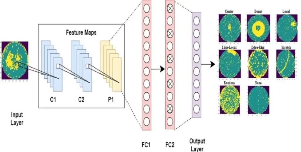
Source: Applied Sciences Journal
Once defects are identified, their information can be semantically mapped into a knowledge graph. In a KG, each defect becomes a node, and its relationships with root causes, process steps, tools, yield implications, and historical patterns are represented as edges.
For example, a bridging defect may be linked to the metal layer and associated with lithography misalignment. This contextual mapping provides a deeper understanding of each defect’s significance and potential origin.
The real strength of this combination lies in the reasoning capabilities of the knowledge graph. By leveraging graph-based learning techniques, the system can trace detected defects back to specific process steps, identify patterns across wafers or lots, and prioritize high-impact anomalies. These insights not only aid in immediate root cause analysis but can also power predictive models that recommend corrective actions. Moreover, such algorithms offer scalability and seamless integration capabilities with existing Automated Optical Inspection (AOI) systems making them suitable for real-world semiconductor manufacturing environments.
yieldWerx Defect Detection with Knowledge Graph Integration
yieldWerx Defect Detection Module improves product quality and reliability by leveraging powerful knowledge graphs to efficiently manage and analyze Metrology/Defect Data. This process allows industry players, especially automotive parts manufacturers to identify yield-impacting issues much faster and more accurately, reducing the cost of quality.
Under the hood, our powerful algorithms powered by knowledge graphs are at play. They help companies save time and money through smart decision-making capabilities. It allows for improved understanding of the relationships between defects, their causes, and their impact on the production process.
Moreover, the Enhanced Data Connectivity offered by this module connects die-level data throughout the entire manufacturing lifecycle, using unique IDs to track and analyze defects from the initial stages to the final test.
Schedule a Live Demo to see our Defect Management module in action.