The concept of GDBN (Good Die in a Bad Neighborhood) is one of the critical aspects of semiconductor manufacturing. This term specifically refers to the occurrence where functional semiconductor dies are surrounded by non-functional ones, presenting a unique challenge in the production process. The effectiveness of GDBN lies in its ability to identify these areas, ensuring that the quality of the semiconductors is not compromised.
Detecting and correcting defects in semiconductor production is crucial for product quality and reliability. A minor deficiency can result in significant functional failures, highlighting the importance of precise defect detection and resolution.
GDBN analysis is critical in this context, as it offers a targeted approach to identify and solve issues on semiconductor wafers.
The Basics of GDBN
GDBN, standing for Good Die/Bad Neighborhood, is a concept central to semiconductor manufacturing. It refers to where functional semiconductor dies (the ‘good dies’) are situated next to non-functional or defective ones (the ‘bad neighborhood’).
The significance of GDBN lies in its ability to pinpoint areas on a semiconductor wafer that may adversely affect the performance and yield of the dies. In an industry where precision is key, understanding GDBN is fundamental to maintaining high product quality standards.
GDBN’s Role in Semiconductor Manufacturing
In semiconductor manufacturing, GDBN plays a key role in quality control and yield improvement. The primary task of GDBN analysis is to examine wafer test results carefully. This involves scanning the wafers to identify patterns and clusters of defects indicative of a ‘bad neighborhood.
These areas are then closely evaluated to determine the impact on adjacent ‘good dies.’ The goal is to ensure that these good dies are not negatively influenced by their surroundings, thereby guaranteeing the functional integrity of the semiconductor products.
Analyzing Wafer Test Results with GDBN
The process of analyzing wafer test results through GDBN involves several steps. Initially, test data from wafers is collected and analyzed to locate defect patterns. This data is important in identifying the specific areas where the ‘bad neighborhoods’ are situated.
Subsequently, engineers use this information to make informed decisions about the viability of the dies in these areas. For instance, if a high concentration of bad dies surrounds a good die, its chances of being defect-free are lower.
Therefore, GDBN analysis not only helps pinpoint defects but also aids in predicting potential future failures, guiding the manufacturing process toward higher efficiency and reduced wastage.
Tools and Techniques for Zero Defects
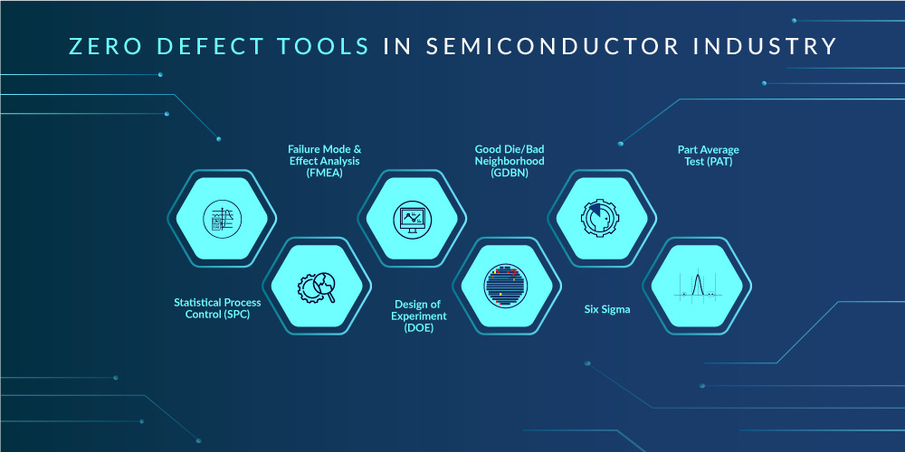
Achieving near-zero defect rates in semiconductor manufacturing is a challenging but essential goal. This objective calls for implementing various tools and techniques that can systematically reduce and eliminate defects in the manufacturing process.
Zero defect tools are essential for maintaining quality standards and ensuring the long-term reliability of semiconductor products.
We will explore some of the most effective tools in this quest for perfection: Statistical Process Control (SPC), Failure Mode and Effects Analysis (FMEA), and Design of Experiments (DOE).
Statistical Process Control
SPC is a method used to monitor and control a process to ensure that it operates at its fullest potential. In semiconductor manufacturing, SPC involves collecting and analyzing data from various stages of the manufacturing process.
This data is then used to identify and correct deviations from the production standards. By continuously monitoring the process parameters, SPC helps maintain process consistency, reducing variability and minimizing defects.
Failure Mode and Effects Analysis (FMEA)
FMEA is a systematic, proactive method for evaluating a process to identify where and how it might fail and to assess the relative impact of different failures. In the context of semiconductor manufacturing, FMEA involves detailed analysis of manufacturing processes to identify potential failure modes, their causes, and their effects on the final product.
By anticipating potential problems, manufacturers can implement corrective actions in advance, thus avoiding the occurrence of defects and improving product reliability.
Design of Experiments (DOE)
DOE is a structured method for determining the relationship between factors affecting a process and the output of that process. In semiconductor manufacturing, DOE is used to systematically test and refine production processes.
Engineers can identify optimal manufacturing conditions that minimize defects by varying process parameters and studying the outcomes. DOE helps understand the complex interactions between various process variables, leading to better process control and a higher yield of defect-free products.
In-Depth Look at GDBN
GDBN focuses on analyzing patterns on semiconductor wafers to distinguish between functional dies and those surrounded by a high concentration of defects.
The process involves a detailed examination of wafer maps. By analyzing these maps, GDBN identifies clusters or ‘neighborhoods’ of dies that are more likely to fail. This analysis is vital for isolating problems and implementing targeted corrective measures, ultimately improving yield and product quality.
Effectiveness in Isolating Issues
GDBN’s effectiveness lies in isolating problematic areas on a semiconductor wafer. By identifying these ‘neighborhoods’ of high failure levels, engineers can focus their attention on specific regions, leading to more targeted and effective problem-solving strategies. This approach helps rectify current issues and guides improvements in manufacturing processes to prevent future defects.
Advanced Pattern Analysis with GDBN
GDBN’s primary function in semiconductor manufacturing is advanced pattern analysis. This technique involves a sophisticated examination of wafer maps to identify clusters of defective dies. By pinpointing these ‘bad neighborhoods,’ engineers can focus on specific areas that are more prone to defects, thereby improving the overall efficiency of the manufacturing process.
GDBN’s Role in Quality Control
In the context of quality control, GDBN is instrumental. It aids in the early detection of potential defects, allowing for timely intervention. This preemptive approach is critical in an industry where even minor defects can lead to significant functional failures in the final product.
Early Detection and Intervention
GDBN’s primary strength lies in its identifying problem areas early. Analyzing the distribution of good and bad dies on a wafer provides a clear picture of where potential defects are likely to occur. This proactive approach allows manufacturers to intervene timely, addressing issues before they escalate into more significant problems.
Minimizing Functional Failures
The importance of GDBN in quality control is underscored by the sensitivity of semiconductor devices. Even small defects can lead to failures in these devices, often used in critical applications across various industries. By effectively utilizing GDBN, manufacturers can significantly reduce the risk of such failures, ensuring the reliability and performance of their products.
Improving Yield and Efficiency
Besides preventing defects, GDBN contributes to manufacturing efficiency. By pinpointing problem areas, it allows manufacturers to focus their resources more effectively, which can lead to improved yield rates. This optimizes product quality and manufacturing processes, making them more cost-effective and efficient.
Supporting Continuous Improvement
GDBN also plays a role in the continuous improvement processes within semiconductor manufacturing. By providing detailed insights into defect patterns, it helps manufacturers understand and refine their processes. This continuous feedback loop is vital for driving ongoing quality control improvement measures.
Complementary Techniques to GDBN

To make GDBN outshine in semiconductor manufacturing, complementary techniques like Six Sigma and Part Average Test (PAT) play a vital role.
In-Depth Integration with Six Sigma
Six Sigma’s detailed approach to minimizing variability complements GDBN’s defect pattern analysis. Six Sigma methodologies, such as DMAIC (Define, Measure, Analyze, Improve, Control), enable a systematic reduction of variations in manufacturing processes.
This structured approach, when aligned with GDBN’s precise defect location identification, boosts the capability to detect and prevent defects. It ensures that the manufacturing process is corrected for current defects and optimized to reduce future occurrences.
Part Average Test (PAT)
Part Average Test (PAT) is an essential counterpart to GDBN. It focuses on the detailed analysis of individual components, identifying outliers that might not be evident in broader testing methods.
When PAT’s detailed individual component analysis is combined with GDBN’s spatial defect pattern recognition, the result is a more nuanced understanding of defects. This amalgamation leads to more efficient identification of problematic areas, significantly reducing the likelihood of defects slipping through manufacturing.
Six Sigma and PAT complement GDBN and uplift its effectiveness in striving for zero defects. They bring a more comprehensive, data-driven approach to quality control in semiconductor manufacturing, ensuring higher product reliability and efficiency.
How yieldWerx™ Facilitates GDBN and Improves Semiconductor Manufacturing?
yieldWerx, with its suite of tools, including GDBN, is designed to address the unique challenges of this sector. The key offerings include Statistical Process Control, which monitors production processes in real-time, and Failure Mode and Effects Analysis, used for identifying potential failure modes early in the product design stage.
Further promoting its capabilities, yieldWerx also incorporates Design of Experiments for testing and analyzing the effects of various factors on processes and products. This is complemented by the implementation of GDBN for analyzing wafer test results to identify defect patterns and the Part Average Test, which evaluates the performance of individual components within integrated circuits.
Integrating tools in yieldWerx enables early detection of defects in semiconductor manufacturing, a field where small issues can significantly impact product functionality. This proactive method, supported by real-time data, optimizes manufacturing for better yields and quality.
GDBN and PAT
Comparing PAT and GDBN methods highlights their distinct approaches to defect detection in semiconductor manufacturing. GDBN utilizes deep learning to analyze labeled and unlabeled data, making it adaptable to new materials and efficient in handling large datasets, yet requiring significant expertise for implementation.

PAT and GDBN methods rely on statistical and spatial analyses to identify outliers and prevent defect clustering, offering a more straightforward application but also needing data analysis skills. Both strategies mark advancements over traditional manual inspections and rule-based systems, demonstrating the semiconductor industry’s shift towards data-driven quality control techniques.
Foreword
The significance of GDBN in ensuring quality in semiconductor manufacturing is paramount. It serves as an important tool in identifying and isolating defect-prone areas on semiconductor wafers, thereby playing an important role in maintaining high-quality standards in producing semiconductor devices.
Adopting a systematic approach to defect identification and resolution is highly recommended for manufacturers.
Tools like GDBN, when used in conjunction with comprehensive solutions like yieldWerx, can significantly optimize the quality control and defect management process.
Frequently Asked Questions (FAQs)
1. What is GDBN in semiconductor manufacturing?
Good Die in a Bad Neighborhood is an outlier detection technique using a die-level neighborhood predictive model. This screening approach uses an algorithmic formula for weighing to eliminate even strong dies that are surrounded by a cluster of failing dies. It also determines the yield of each die.
2. How does GDBN contribute to identifying manufacturing defects?
GDBN helps identify patterns of defective dies on a wafer. Analyzing these patterns isolates areas with high defect concentrations, enabling targeted interventions to address and resolve these defects effectively.
3. Can GDBN work in isolation or require complementary tools?
While GDBN is effective, it often works best alongside other tools and methodologies. Complementary tools can provide a more comprehensive understanding of the manufacturing process and help address a wider range of potential issues.
4. What are some common challenges in implementing GDBN, and how does yieldWerx address them?
Implementing GDBN can be challenging due to the complexity of semiconductor manufacturing processes. yieldWerx addresses these challenges by providing an integrated suite of tools and outlier detection techniques, including GDBN, which simplifies the defect identification and resolution process.
5. How can manufacturers integrate GDBN and yieldWerx into their existing systems?
Manufacturers can integrate GDBN and yieldWerx by adopting the yieldWerx Enterprise solution, which is designed to be compatible with various semiconductor manufacturing processes.


