The semiconductor industry has come a long way from the days of simply sorting “good units” from “bad units.” Today, yield analysis dives deep into data science, uncovering many factors that affect production. With manufacturing defects as old as the integrated circuit itself, the modern era introduces even more complexities through design, process, and market dynamics. Addressing these challenges requires advanced yield optimization capabilities, powered by modern data analytic architectures utilizing artificial intelligence (AI) and machine learning (ML).
Explaining the Semiconductor Yield
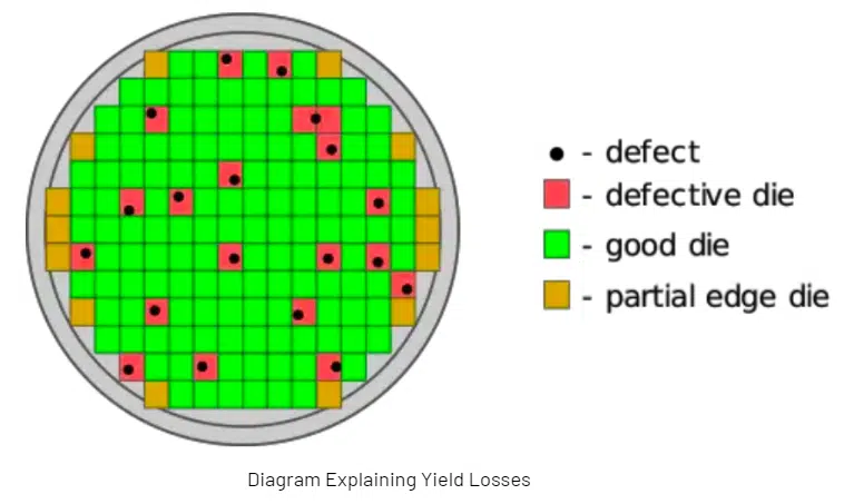
In semiconductor manufacturing, a single silicon wafer contains tens to hundreds of microelectronic integrated circuit units, known as dies. Each wafer undergoes numerous manufacturing steps, involving advanced tools processes.
Problems can arise, such as tool failures, mismatched tool operations, or unintended impacts from one processing step on another. These issues introduce variability in the manufacturing line, which can negatively affect the end-of-line yield resulting in ‘yield losses’.
Considering there are 260 dies per wafer and around 18 defective dies per wafer, therefore the yield is 93%. Let’s assume this product is produced at a volume of 200 wafers per month where the yield is 93% and each wafer costs $6000 from the foundry.
If you can improve this number to 98% using modern data analytics schemes you will save $60,000 per month or $720,000 a year just on that product while delivering the same number of good die to your customers.
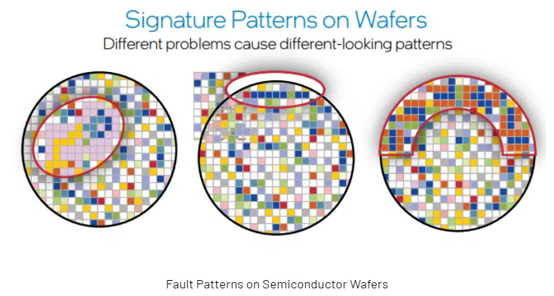
Yield analysis engineers meticulously inspect end-of-line wafers for die-level health indicators and outliers. A critical part of their job is identifying gross failure areas (GFAs), which manifest as distinct patterns signaling problems in the fabrication process. Each pattern tells a story, hinting at specific issues that need addressing.
Until recently, engineers relied heavily on manual pattern recognition techniques to piece together these clues, driving the root cause analysis process. Now, as we stand at the brink of a new era, advanced data analytics approaches promise to revolutionize yield management solutions, offering unprecedented insights and solutions.
Issues With The Traditional Yield Management Approach
Time-consuming
GFA detection in semiconductor manufacturing is a repetitive and labor-intensive task. As product volumes grow, it becomes impractical to hire enough yield engineers to review all end-of-line material, making the manual approach time-consuming and non-scalable due to human resource constraints.
Highly Dependent on the Level of Engineering Expertise
Yield analysis engineers need many years to gain the necessary experience, as GFA detection is a blend of art and science that requires the skill to distinguish between random noise and actual patterns. As a result, the accuracy and consistency of analysis depend heavily on the engineer’s expertise. New issues not matching baseline patterns may go undetected until noticed by experienced engineers, leading to delayed issue detection.
Struggles to Handle Multiple Problems Simultaneously
Furthermore, multiple inline problems can result in several patterns on a single wafer. Due to resource and experience limitations, engineers may identify only one issue, leaving others unresolved, which hinders the ability to fix the root causes of all issues.
Modern Techniques For Enhancing Semiconductor Yield And Quality Control
The good thing here is that with the level of automation in modern fabs extensive production data spanning over years is readily available. Therefore, semiconductor companies are integrating AI, ML, computer vision, and other technologies to develop intelligent manufacturing environments. The primary goals of using AI technologies are to reduce costs, save time, improve quality control, and increase the robustness of industrial processes.
Understanding Supervised Vs. Unsupervised Learning
Supervised learning techniques utilize real-world input and output data for outlier detection. These systems require a data analyst to label data points as either normal or abnormal, which are then used as training data.
In contrast, unsupervised learning techniques do not need labeled data and can manage more complex datasets. Powered by deep learning, neural networks, or autoencoders, unsupervised learning mimics the signaling processes of biological neurons in the human brain.
Benefits of Using AI/ML for Semiconductor Yield Management Systems
1) Enhanced Pattern Recognition
AI can identify and document multiple gross failure areas per wafer, and learn to capture yield-affecting patterns faster while consuming fewer resources. Computer vision and AI algorithms enhance wafer testing by detecting defects in both front-end and back-end production processes using advanced cameras and microscopes and that too with minimal human intervention. Intel is already doing it with great success.
Utilizing dedicated hardware, such as GPUs and TPUs, along with on-premises edge computing, enables real-time, scalable training and deployment of computer vision algorithms.
A study investigates using high-quantized neural networks to be implemented on small industry-grade microcontrollers enhanced with hardware accelerators. The system proposes an automatic visual inspection and classification of defects in both the front- and back-end manufacturing processes in the semiconductor industry to increase yield and reduce costs.
2) Accurate Yield Prediction
In semiconductor manufacturing, accurately forecasting yield is crucial for enhancing productivity and profitability. However, achieving reliable wafer yield forecasts presents significant challenges.
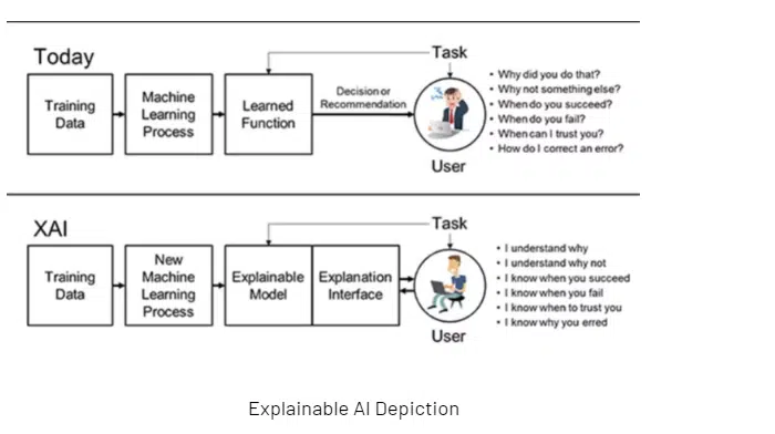
This challenge can be addressed by adapting explainable artificial intelligence (XAI) that uses model interpretation to modify fab conditions. The goal of XAI is to make the rationale behind the output of an algorithm understandable by humans, ending the black box nature of AI systems and enhancing scrutiny.
Engineers can utilize a cascading classifier approach to translate the production process into a cascading quality forecasting procedure. With the help of individualized machine learning algorithms for each process step, it is possible to determine which results the wafer will produce when it passes through the next process steps. These predictive data can then be compared to the real data after each process step to evaluate the success.
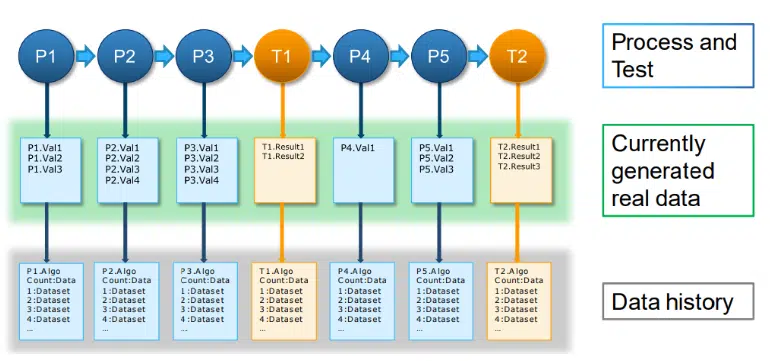
Overall, a product predicted as not having a good yield can be specially observed and managed, and the yield prediction function can be integrated into a platform.
3) Predictive Maintenance
Predictive maintenance outperforms traditional maintenance methods by utilizing telemetry data from physical sensors, process variables, and product metrology. This approach predicts when maintenance is required and provides a time window to address potential issues before a failure occurs.
AI enhances semiconductor manufacturing process and predictive maintenance, resulting in quality output and improved yields. AI-enhanced predictive maintenance can improve equipment uptime with increases of around 10-20 percent, reduce the time spent planning maintenance by up to 50 percent, and reduce material spend by 10 percent. This would have the effect of reducing overall maintenance costs by 10 percent; a potential saving of millions of dollars for large companies.
Companies can use various ML techniques on computational data collected from the sensors in semiconductor manufacturing units to predict maintenance requirements. Numerical results clearly show that such methods can be implemented to predict wafer failure, perform predictive maintenance, and increase manufacturing efficiency.
4) Anomaly Detection
ML-based approaches for anomaly detection have proven to be extremely effective in increasing anomaly detectability and, in general, in enhancing monitoring procedures. Yield researchers have successfully developed outlier detection methods that can even work with only a small amount of labeled data to begin with.
In semiconductor manufacturing, vast amounts of time series data are quickly collected from equipment sensors, making it challenging to identify abnormal signals. This data includes multiple variables of varying lengths and often has a skewed ratio between abnormal and normal signals. Due to these characteristics, conventional rules-based techniques, like excursion detection methods, may not be suitable for the task.
Conclusion
While AI and machine learning offer transformative potential for semiconductor manufacturing, there are several challenges to overcome. These systems can only detect faults based on the data they are trained on, which means they may struggle with unexpected anomalies. They also require substantial amounts of data for training and need to be adaptable to specific customer needs. Integration of AI presents challenges related to ensuring data quality, computational capacity, and cultural shifts within wafer fabrication facilities.
Traceability throughout the semiconductor lifecycle is crucial for effective AI-driven analytics, and human expertise remains essential to guide AI/ML algorithms and refine models. Additionally, current industry resistance to data integration hampers the full potential of AI/ML.
However, despite these challenges, AI/ML enables proactive maintenance and real-time process adjustments, enhancing decision-making by democratizing data visualization and breaking down departmental silos. With ongoing investments in AI/ML, the efficiency and effectiveness of semiconductor manufacturing are set to improve significantly in the near future.
Here are some of the key questions that effective AI/ML-assisted yield management software should be able to answer in minutes instead of hours or days.
- What is the current yield, and how has it trended throughout the quarter?
- Is the yield consistently uniform across the wafer? If not, what factors contribute to the variations?
- Which bins and tests have the highest failure rates, and what trends can be observed with these failures?
- Are the tested parameters sensitive to the test software or hardware?
- What impact is Fab having on the wafer sort and final test yields?
If your engineers are struggling to extract and report the right data pinpointing the root cause of yield losses, then it’s time to switch to a better solution.
yieldWerx delivers a cutting-edge yield management system, harnessing AI and ML to boost semiconductor yield. Enjoy the advantages of accurate root cause analysis, reduced site-to-site variations, and minimized scrap. Contact us today to unlock the full potential of your data.
List of References
- Explainable AI: What is it? How does it work? And what role does data play?
- DELOITTE-Predictive maintenance and the smart factory
- Transforming Semiconductor Yield Management with AWS and Deloitte
- Dealing With AI/ML Uncertainty
- Anomaly detection in machine learning: Finding outliers for optimization of business functions
- INTEL: Transforming Manufacturing Yield Analysis with AI
- Efficient Deep Learning Approach for Fault Detection in the Semiconductor Industry
- Optimal Predictive Maintenance Technique for Manufacturing Semiconductors using Machine Learning
- Yield prediction in semiconductor manufacturing using an AI-based cascading classification system