
When it comes to semiconductor data analytics, pinpointing the unusual is not just about finding a needle in a haystack; it’s about understanding how that needle can skew the entire stack. Outlier detection stands at the forefront of ensuring data integrity, directly influencing the yield and performance of semiconductor products.
Whether you’re determining outliers to refine quality control processes or exploring outlier detection methods to innovate new testing strategies, the significance of accurate and efficient outlier detection cannot be overstated.
Understanding the Impact of Outliers in Semiconductor Data Analysis
An outlier is a value that significantly differs from the other data points in a dataset. In the context of semiconductor manufacturing, these are the anomalies that, if not identified and addressed promptly, can skew the entire analysis, leading to incorrect conclusions and, more critically, impacting the yield and performance of semiconductor products. yieldWerx’s data analytics and yield management solutions are designed to navigate through the data, applying advanced outlier detection tests and guaranteeing that each data point contributes to a reliable analysis.
Accurate outlier detection is not just about identifying the anomalies; it’s about understanding their impact, tracing their origins, and taking informed actions to mitigate their effects.
Technique 1: Standard Deviation Method

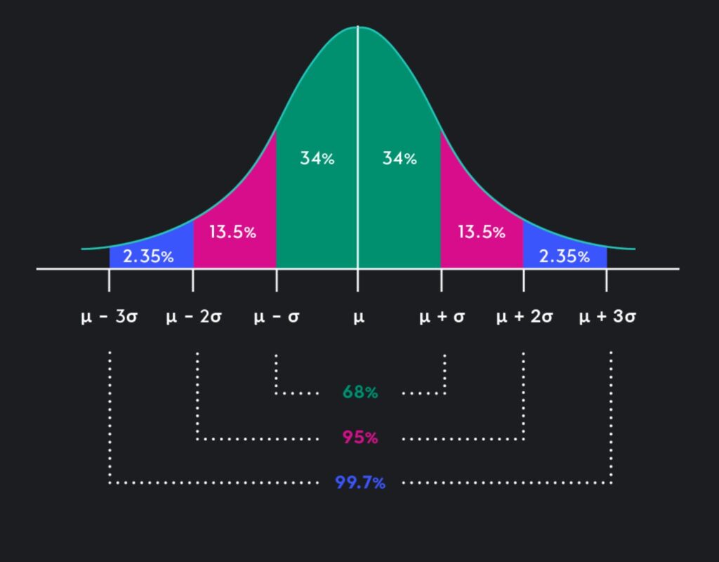
The Standard Deviation Method is pivotal in outlier detection, providing a statistical basis to identify abnormal data points within a dataset. Centered on standard deviation, this method quantifies how much data points vary from the average. For semiconductor data analysis, applying this method is crucial for upholding data accuracy and consistency.
Functionally, the Standard Deviation Method flags outliers by highlighting data points that deviate significantly from the mean, typically those beyond two standard deviations.
Technique 2: Machine Learning-Based Anomaly Detection

Machine Learning-Based Anomaly Detection represents a significant leap in identifying outliers within complex data structures. By harnessing advanced algorithms, this approach can discern subtle patterns and irregularities, efficiently pinpointing anomalies that could potentially disrupt semiconductor manufacturing processes. Its adaptability and learning capability make it particularly suitable for dynamic datasets, where traditional static methods might falter.
This innovative method ensures a high level of precision in outlier detection and evolves with the data, continually enhancing its detection capabilities as it processes more information.
Technique 3: Multivariate Analysis (MVA)

Multivariate Analysis (MVA) is a critical technique in outlier detection. It offers a comprehensive framework for analyzing data with multiple variables. Its ability to handle complex, multidimensional datasets makes it invaluable for spotting anomalies that might not be detectable when examining variables individually.
In the semiconductor industry, where intricate relationships between numerous variables can significantly influence product quality and manufacturing processes, MVA’s capacity to dissect and interpret multivariate data structures is crucial in maintaining high standards of precision and efficiency.
Case Study: Multivariate Analysis (MVA) in Semiconductor Industry
The study highlights the role of Multivariate Analysis (MVA) in improving semiconductor manufacturing through smart manufacturing techniques. It combines systems to unite physical and digital capabilities, utilizing big data to improve manufacturing operations.
MVA is key to improving yield levels, speeding up new product phases to high-yield status, and minimizing waste. The emphasis on data quality and the integration of expert knowledge in analytics underscore the importance of strategic data analysis in modern manufacturing, ensuring data-driven decisions bolster the industry’s competitiveness and efficiency.
Technique 4: Wafer Map Pattern Recognition
Wafer Map Pattern Recognition is crucial in the semiconductor industry. It is a sophisticated approach to detecting outliers and anomalies in wafer data. This method involves analyzing spatial patterns on wafer maps and identifying irregularities that may indicate defects or inconsistencies in the manufacturing process.
It’s particularly valuable in ensuring the quality and reliability of semiconductor products, as it facilitates the early detection of issues, allowing for timely intervention and corrective actions.
Case Study: Wafer Map Pattern Recognition in Semiconductor
In the case study featured in IEEE Transactions on semiconductor manufacturing, Wafer Map Pattern Recognition is a crucial tool for maintaining the integrity and performance of semiconductor wafers. This technique utilizes spatial correlogram to detect spatial autocorrelations and the dynamic time-warping algorithm to classify spatial patterns on wafer maps automatically.
The application of spatial correlogram and dynamic time warping in Wafer Map Pattern Recognition allows for an in-depth understanding and effective categorization of defect patterns, which is pivotal in diagnosing and rectifying process-related issues.
Technique 5: Physics-Based Modeling
Physics-based modeling marks a strategic advancement in semiconductor manufacturing, especially in the domain of outlier detection. This approach is grounded in the fundamental laws of physics, offering a profound understanding of how various parameters converge, diverge, and influence the manufacturing process by accurately simulating the interactions within a system.
This depth of insight is critical for identifying and rectifying anomalies in semiconductor operations. Unlike surface-level statistical methods, this technique delves deep into the physical interactions, ensuring that the identified outliers are not just statistical deviations but are rooted in the underlying physical processes.
Case Study: Adapting Physics-Based Modeling in Semiconductor
In a groundbreaking study featured at the ASME 2020 International Mechanical Engineering Congress and Exposition, a sophisticated blend of System Dynamics (SD) and Discrete Event Simulation (DES) within Physics-Based Modeling emerges as a transformative force in the realm of cyber-physical manufacturing systems. This innovative approach integrates DES for discrete process modeling with SD components.
The study demonstrates the model’s proficiency in detecting anomalies and elucidating their underlying causes within a commercial discrete manufacturing setup, marking a significant stride in manufacturing process optimization.
Technique 6: IQR (Interquartile Range) Technique
The Interquartile Range (IQR) technique is a statistical method crucial for detecting outliers, especially in datasets with skewness or extreme values. The IQR measures the spread of the middle 50% of a dataset, calculated as the difference between the 75th percentile (Q3) and the 25th percentile (Q1) of the data.
This method is highly valued in the semiconductor industry for its robustness, as it is less sensitive to extreme values than other measures like variance or standard deviation. By focusing on the central spread of the data, the IQR technique provides a clear picture of data distribution, making it easier to identify and handle outliers effectively.
Case Study: Using IQR for Improved Semiconductor Quality
In a practical application shared by Analytics Vidhya, the IQR method was employed to address outliers in a dataset, demonstrating its effectiveness in improving data quality and reliability. The study involved a visual comparison of distribution plots before and after data trimming, revealing a noticeable difference in the data’s distribution.
The use of boxplots revealed that nearly 99% of the outliers were removed after applying the IQR method. Additionally, the technique of ‘capping’ was used to impute the outliers with other values, ensuring no data was lost. The analysis confirmed that the data remained within the set range of the upper and lower limits defined by the IQR technique.
Post-capping, the dataset showed no presence of outliers, indicating a successful application of the IQR method in enhancing data quality and consistency.
Technique 7: Box Plot Analysis
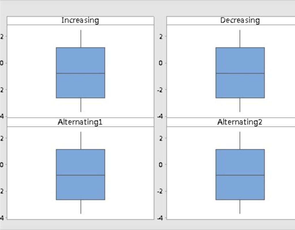
Box Plot Analysis is a powerful visual outlier detection and data distribution assessment tool. This technique graphically depicts groups of numerical data through their quartiles, highlighting the median, upper, and lower quartiles and any outliers in the dataset. In the semiconductor industry, where precision is paramount, Box Plot Analysis offers a clear and concise way of identifying data points that deviate significantly from the rest, aiding in the swift detection and rectification of any abnormalities that could affect the overall process and product quality.
In industries where precision is paramount, such as semiconductor manufacturing, the ability to interpret and act on data insights can significantly drive process improvements and quality enhancements, underscoring the indispensable role of Box Plot Analysis in data-driven decision-making.
Technique 8: Z-Score Method
The Z-Score Method is a statistical technique used for outlier detection, gauging how far a data point is from the mean of a dataset in terms of standard deviations. This method converts data points into a standardized form, allowing for comparing data from different sets or scales.
By standardizing data and pinpointing outliers with high precision, the Z-Score Method effectively filters out noise from the data set, allowing engineers and analysts to focus on the most relevant information.
Case Study: Enhancing Operational Efficiency with the Z-Score Method
The study examines Altman Z-score’s predictive ability and theoretical and empirical limitations, and it introduces a rough set approach to enhance financial ratio analysis for distressed firms. This method offers improved financial insight, notably highlighting the decline in profit efficiency in Taiwan’s solar energy sector. The research validates the Z-score’s utility in boosting operational efficiency and decision-making, demonstrating its importance in financial analysis and industry optimization.
Technique 9: DBSCAN (Density-Based Spatial Clustering of Applications with Noise)
DBSCAN is a standout method for outlier detection, especially proficient in managing large datasets with complex structures and noise. This method autonomously discerns the number of clusters in a dataset, which sets it apart from other clustering techniques that typically require predefined cluster counts. By identifying and evaluating dense regions of data points, separated by areas of lower density, DBSCAN effectively isolates outliers from the main clusters.
This ability to distinguish subtle differences and irregularities in data makes DBSCAN an invaluable tool in fields that demand rigorous data analysis, such as comprehensive yield analysis. Its application ensures that every data point is assessed, offering a detailed and accurate understanding of data patterns and anomalies.
Case Study: Implementing DBSCAN for Comprehensive Yield Analysis
DBSCAN’s prowess in enhancing active learning through Convolutional Neural Networks (CNN) was explored for defect classification in the semiconductor industry. The study focused on deploying CNN models for chip defect classification in semiconductor wafers.
Utilizing DBSCAN, the framework aimed to optimize the active learning process by querying the most informative samples based on uncertainty estimation and employing density-based clustering to refine the queried images. This approach significantly minimized manual labor by ensuring only the most representative images were passed for labeling.
Technique 10: Local Outlier Factor (LOF)
The Local Outlier Factor (LOF) is an analytical tool that identifies anomalies within data sets. This method significantly contributes to identifying data points that substantially deviate from the norm, providing a nuanced perspective on datasets. By evaluating the local density variation of a data point concerning its neighbors, LOF serves as a robust mechanism, especially in environments where precision and accuracy are paramount, such as in semiconductor manufacturing.
LOF’s capability to detect outliers in a localized context makes it an indispensable tool in quality control and process optimization.
Case Study: Local Outlier Factor (LOF) for Accurate Outlier Detection
In the case study highlighted in recent industrial research, implementing the Local Outlier Factor (LOF) method in semiconductor manufacturing underscored its capability as a sophisticated outlier detection mechanism. When applied to the intricate processes involved in semiconductor fabrication, this approach demonstrated a marked ability to identify and isolate aberrations, thereby safeguarding the integrity of the production process.
Improving Semiconductor Quality with yieldWerx Outlier Detection
yieldWerx introduces advanced outlier detection techniques like Part Average Testing (PAT) and Good Die Bad Neighbour (GDBN) to meet these industry challenges. These methodologies enable early detection of anomalies, which is vital for maintaining high standards in semiconductor production.
PAT (Part Average Testing)
PAT employs statistical data from previously measured parts to set test limits, effectively identifying devices that deviate from expected behavior. This advanced method ensures accurate anomaly detection in semiconductor manufacturing, improving quality control.
GDBN (Good Die Bad Neighbour)
GDBN focuses on detecting defects in clusters by analyzing the yield of individual dies. Employing an algorithmic approach, it identifies potentially good dies near failing ones, offering a granular level of quality assurance in the manufacturing process. Explore our solutions today.
Conclusion
In semiconductor data analytics, accurately detecting outliers for quality improvement in semiconductor testing is more than finding anomalies; it’s about grasping their influence on the entire data set and, consequently, on product yield and performance. Techniques such as Standard Deviation, IQR, Box Plot Analysis, Z-Score, and DBSCAN are integral to maintaining data accuracy in semiconductor manufacturing. These methods do not just spot the irregularities but delve deep into their origins and implications, guiding industry professionals in their strategic decision-making.
Amid these sophisticated techniques, yieldWerx positions itself as a cornerstone of innovation in data analytics and yield management. Embrace the advanced solutions and embark on a transformative path towards overcoming the challenges in semiconductor yield management, driving success through precision and insight.


