Chiplets: The Building Blocks of Sustainability
Leading semiconductor companies are increasingly adopting circularity principles to extend the lifecycle of their products. These strategies aim to divert materials from final disposal through recycling, repair, resale, or reuse. The recent Chiplet Summit held in Santa Clara underscored this shift, spotlighting how modular chiplet architectures are not only advancing performance but also enabling more reusable systems. Heterogeneous Integration (HI) systems hold strong promise for advancing sustainable computing by reducing carbon emissions through two main strategies:
- Reusing pre-designed chiplet IP blocks.
- Adopting hierarchical system design.
This is happening because key markets are implementing tough regulations that tie environmental performance and transparency directly to market access and competitiveness. At the same time, stakeholder expectations have grown significantly. Customers now routinely expect their semiconductor suppliers to align with clearly defined sustainability goals and demonstrate measurable progress.
By leveraging existing chiplets across multiple products and even across successive generations of integrated circuits, manufacturers can significantly cut down on design, testing, and fabrication overhead. Ultimately, this leads to a reduction in carbon footprint across the entire product lifecycle.
In this blog post, we’ll explore the top sustainability challenges facing the semiconductor industry and how chiplet-based architectures are crucial to enabling circularity. We’ll also examine how yield management solutions like yieldWerx are leading the way in reducing silicon waste and supporting the green economy.
Three Barriers to Semiconductor Sustainability
The semiconductor industry faces three major types of waste that impact both costs and environmental sustainability:
1. Silicon Waste from Yield Loss
Silicon wafers are the foundational material upon which semiconductors are built. During fabrication, each wafer undergoes numerous high-precision steps to create hundreds or thousands of dies (individual chips). However, not all dies pass quality testing due to random defects introduced during processing, alignment errors, contamination, or design-process mismatches.
These failed dies represent wasted silicon, materials, and process effort. According to a study by Chen et al. published in MDPI Processes, it’s estimated that as much as 50% of a silicon wafer can be lost due to these failures, especially when producing advanced-node or high-complexity chips. This kind of inefficiency becomes even more critical as complexity grows and chip sizes shrink, as margins for error become razor-thin.
2. Energy-Intensive Manufacturing
Semiconductor fabrication is among the most resource- and energy-intensive manufacturing processes in the world. From maintaining ultra-clean cleanrooms (Class 1 or better), to powering EUV photolithography machines, and to the use of specialized gases and chemicals for etching and deposition—every step consumes vast amounts of energy.
A single advanced fab can consume hundreds of megawatts of power and millions of gallons of ultrapure water per day. This not only raises the carbon footprint of chip production but also places stress on local utilities and water supplies, especially in regions prone to drought or limited infrastructure (e.g., Taiwan, Arizona).
3. Premature Obsolescence and E-Waste
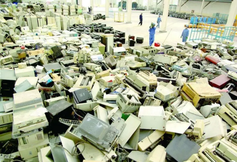
Consumer electronics—such as smartphones, laptops, TVs, and even appliances—are often designed with short product lifespans. Manufacturers release frequent updates, and software ecosystems often drop support for older hardware, pushing users to upgrade regularly. As a result, functional semiconductor components are often discarded while still usable. This phenomenon, known as premature obsolescence, fuels the global e-waste crisis.
A record 62 million tonnes (Mt) of e-waste was produced in 2022. The number is rising by 2.6 million tonnes annually. Less than one quarter (22.3%) of that year’s e-waste mass was properly collected and recycled.
Recovering high-value materials from semiconductor packages is difficult due to the use of tiny, tightly bonded elements and mixed materials. Consequently, discarded electronics end up in landfills or informal recycling operations, causing pollution and health risks.
What is a chiplet?
Why does it matter as we approach the end of Moore’s law?
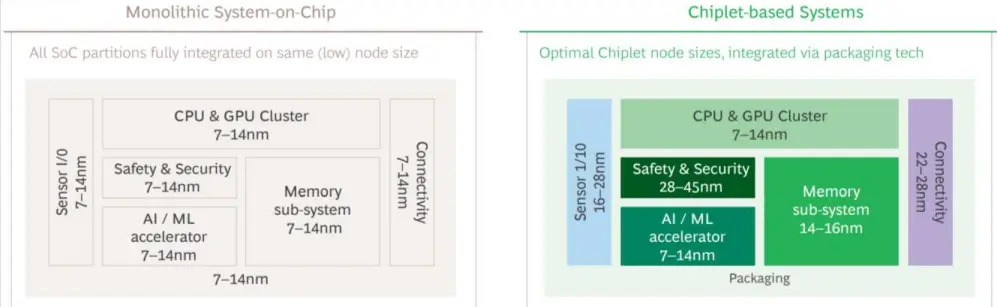
Chiplets are individual semiconductor units that can be combined to create a complete system-on-a-chip (SoC) or a more complex semiconductor device. Each chiplet can be manufactured separately and then assembled onto a substrate or package enabling targeted enhancements in specific areas like processing power, memory, or specialized functions. These chiplets communicate with each other over high-speed, standardized interconnects, e.g. UCIe and BoW, allowing designers to meet size, power, performance, efficiency, and cost challenges in the Internet of Things (IoT), AI, and VR era.
Moore’s Law, which predicts that the number of transistors on a chip would double approximately every two years, can no longer be sustained due to physical limitations in miniaturizing transistors. As the size of transistors approaches the atomic scale, it becomes more difficult and expensive to continue scaling down silicon features.
Here’s why chiplet-based design is the game-changer in the current scenario:
Boosting Yields:
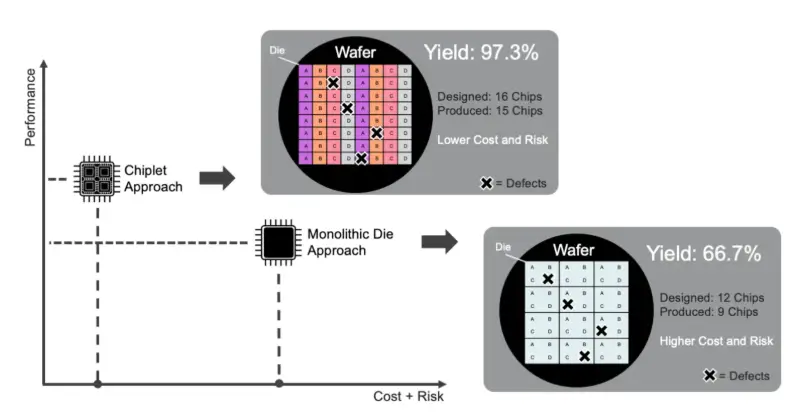
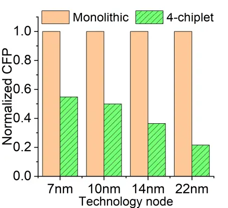
Chiplet designs reduce costs by using mature process technologies. If a single chiplet fails, only that piece is discarded, preserving the integrity of the entire system and boosting overall yield. This becomes increasingly crucial as die sizes grow and process nodes shrink.
For example, splitting a 400 mm² monolithic die into four 100 mm² chiplets improves yield from ~50% to ~90% in advanced nodes due to the inverse relationship between die area and yield.
Pre-testing chiplets before assembly ensures only defect-free units are used. It is called the Known Good Die (KGD) phenomenon.
Breaking the Limits of Scaling:
As transistor sizes near their physical limits, monolithic designs struggle to keep pace with growing performance demands. Chiplets are optimized for specific tasks, overcoming the scaling challenges and unlocking new performance potential.
Tailored for Innovation:
With chiplets, designers can create specialized modules like processors, memory, and I/O interfaces, all fine-tuned for their intended purposes. This modular approach offers unmatched flexibility, enhancing both performance and power efficiency.
Seamless Integration of Diverse Technologies:
Chiplets open the door to heterogeneous integration – combining different technologies or process nodes (e.g., cutting-edge logic chiplets with older memory chiplets) to harness the best technology for each function. It’s the ultimate mix-and-match for optimal performance.
Rising Above Moore’s Law:
As we near the end of Moore’s Law, heterogeneous integration based on chiplets offer a sustainable solution. Instead of relying solely on shrinking transistors, chiplets enable performance boosts through innovative architectures, improved interconnectivity, and specialized processing units – ensuring continued growth in computing power.
Known Good Die
In chiplet architecture, the concept of a Known Good Die (KGD) refers to ensuring that each individual chiplet has been fully tested and verified as functional before it is assembled into a larger multi-chip module (MCM) or system-in-package (SiP).
This concept is crucial because, unlike monolithic chips, chiplet-based designs integrate multiple smaller dies—often manufactured using different processes or technologies—which increases the risk of failure if any single chiplet is defective.
By validating each chiplet in advance, manufacturers can significantly reduce assembly waste, improve overall yield and reliability, and enable scalable, modular system designs. KGDs support heterogeneous integration, allowing designers to combine specialized components (such as memory, logic, or analog blocks) with greater flexibility.
Analog functions—such as power converters and sensors—typically do not require cutting-edge technology nodes; in fact, they often perform better when built on larger, more mature geometries. These established process nodes offer greater stability and are substantially more cost-effective to manufacture. However, achieving KGD status involves rigorous wafer-level or die-level testing, and sometimes stress testing, which can be technically challenging and add to manufacturing costs.
Open Chiplet Economy For Semiconductor Sustainability
The Open Chiplet Economy refers to an emerging semiconductor design and manufacturing model where chiplets can be sourced, mixed, and integrated from different vendors using open standards and interfaces. This model promotes interoperability, modularity, and innovation, similar to how components like RAM or GPUs can be interchanged in traditional computing systems.
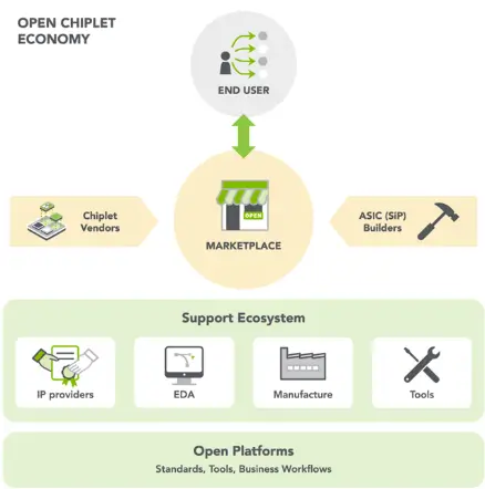
By reusing verified, known-good chiplets, the open chiplet economy reduces development costs, accelerates time-to-market, and supports semiconductor sustainability. This shift is particularly important as Moore’s Law slows and monolithic chip designs become increasingly expensive and complex.
Major initiatives from the UCIe Consortium, DARPA’s CHIPS program, and organizations like CHIPS Alliance and the Open Compute Project are driving the adoption of this modular, scalable design paradigm.
Open standards foster competition and collaboration across the industry, encouraging eco-efficient designs and greener supply chains. With shared tooling and platforms, smaller players can develop energy-efficient chiplets without the need for massive capital expenditure.
Smarter Chips, Smaller Footprint: How Chiplet Architectures Drive Circularity
Chiplet-based architecture addresses above mentioned semiconductor industry waste streams in the following ways:
1. Reducing Carbon Footprint through Modularization
AMD recently evaluated the sustainability impact of using chiplet-based design in its wafer manufacturing process—and the findings are striking. By producing its 4th Gen EPYC CPUs with eight smaller compute chiplets instead of a single monolithic die, AMD avoided manufacturing enough wafers to reduce approximately 50,000 metric tons of CO₂e in 2023—equivalent to its entire operational carbon footprint for 2022.
Traditional monolithic chips are discarded entirely if even one section is defective, wasting otherwise functional silicon. Chiplets solve this by breaking the chip into smaller, independently manufactured and tested components. If one chiplet fails, it can be replaced without scrapping the whole unit. This modular approach significantly improves yield and carbon footprint.
2. Power and Thermal Gains from Chiplets
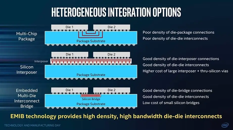
In monolithic designs, long interconnects can lead to significant power loss. Chiplets, connected via advanced packaging techniques like silicon bridges or interposers, enable shorter and more efficient interconnects. This design reduces the capacitive load and, consequently, the power required for data transmission between components.
Chiplet architectures can be designed to distribute heat more evenly across the package, reducing hotspots. Better thermal distribution allows components to operate at optimal temperatures, improving performance stability. The modular nature of chiplets enables dynamic power management strategies, such as powering down unused chiplets during low-demand periods. This flexibility contributes to overall energy savings in various workloads.
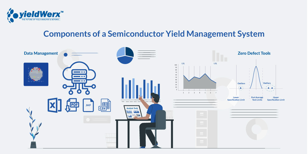
3. Yield Management Systems for Sustainable Chiplet Integration
As chiplet systems become more complex, managing their quality and interactions requires robust yield management systems. These systems:
- Track manufacturing and test data across different chiplet types and fabs.
- Correlate cross-chiplet defect patterns to identify root causes of failure (e.g., a specific interconnect or packaging issue).
- Ensure that only KGDs are integrated into the final system.
This process also supports bin optimization and predictive analytics. Ultimately, this enhances supply chain efficiency and environmental responsibility by minimizing rework, shipping failures, and field returns.
4. Lifecycle Extension and E-Waste Reduction
Chiplet-based systems can be designed for partial upgrades or replacements, where outdated or failed chiplets are swapped while the rest of the package remains in service. For example, you could update the AI accelerator chiplet in a data center SoC without replacing the memory or I/O components. This modularity:
- Extends the lifespan of semiconductor systems.
- Reduces total electronics waste by limiting full-package disposal.
- Improves semiconductor reuse and recycling, especially when paired with open standards.
- Reduces reliance on virgin resources leading to increased circularity.
Barriers to Sustainable Adoption of Chiplet Architecture
While chiplet architectures offer promising pathways to improve efficiency and reduce e-waste, several technical, logistical, and economic challenges must be addressed to ensure that chiplets contribute meaningfully to circular economy goals. This section outlines key barriers that currently limit the sustainable adoption of chiplet-based systems.
Complex Packaging and Assembly
Chiplet systems rely on advanced packaging technologies which are more complex and resource-intensive than traditional methods. These processes can offset some of the energy and material gains made through modularization if not optimized.
Limited Standardization Across Ecosystem
The lack of widely adopted open standards for chiplet interfaces–such as the still-maturing UCle–UCIe still maturing) makes interoperability difficult. This limits reuse and component interchangeability, both of which are critical for achieving circular economy goals.
Testing and KGD Validation
Ensuring every chiplet meets strict KGD standards is challenging. Additional test steps and equipment increase costs and energy consumption if not well-integrated into yield management systems.
Data Silos in Yield and Failure Analysis
Chiplet manufacturing often involves multiple fabs and suppliers. Disjointed data across the supply chain can make it difficult to trace defects and optimize for yield, potentially increasing waste due to misaligned process parameters.
Limited Support for Lifecycle Extension
While modularity enables upgrades and reuse, most current chiplet designs are not yet built with long-term upgradability or recyclability in mind. Reverse logistics, partial replacement, and recycling processes are still underdeveloped.
Higher Initial Resource Demand
The startup phase of chiplet adoption may involve more R&D, new equipment, and energy use before sustainable gains are realized at scale.
Economic Viability and Industry Adoption
For smaller companies, the upfront investment in chiplet-based design and packaging may not be justifiable, which can slow the broader adoption needed for large-scale environmental impact.
yieldWerx for Chiplet-Driven Innovation
yieldWerx offers scalable, data-driven yield management solutions tailored to companies of all sizes, including emerging chiplet design companies. yieldWerx modules provide advanced capabilities such as KGD tracking, die-level yield correlation across multi-fab supply chains, and defect pattern recognition.
Its customizable dashboards and workflows empower engineers to focus on the unique challenges of chiplet architectures, while tiered licensing and dedicated onboarding support make the platform accessible to smaller players.
Bring Circularity and Sustainability to Your Semiconductor Manufacturing Processes.
Contact Us For a Free Consultation and Learn How yieldWerx Helps You Track, Test, and Improve Chiplet Performance.
List of References:
- Recovery of Valuable Materials from the Waste Crystalline-Silicon Photovoltaic Cell and Ribbon
- UNITAR: The global E-waste Monitor 2024
- Chiplet Technology: Revolutionizing Semiconductor Design- A Review
- Hybrid chips to enable a sustainable internet of things technology: opportunities and challenges
- What Is A Chiplet, And Why Should You Care?
- Chiplet Heterogeneous Integration Technology—Status and Challenges
- Open Chiplet Economy
- ECO-CHIP: Estimation of Carbon Footprint of Chiplet-based Architectures for Sustainable VLSI
- Thinking Small to Think Big: AMD Modular Architecture is Advancing Sustainability
- HPC, chiplets and interposers
- Circularity of Semiconductor Chip Value Chains: Advancing AI Sustainability Amid Geopolitical Tensions
- Semiconductor sustainability: New life through circularity
- Test & Yield Challenges of Chiplet-Based Semiconductor Products

