
How to Deal with the Challenges of MEMS Test Data Management and Yield Analysis
MEMS (MicroElectroMechanical Systems) are marvels of modern engineering. They blend mechanical and electrical components to enable advanced technologies like LiDAR, medical imaging, accelerometers, microphones, and pressure sensors. While their design inspires awe, the journey from concept to production is fraught with challenges.
MEMS testing is limited in scope by the different stimuli and measurements needed for various products with overall test costs remaining high. These stimuli can come in the form of temperature, sound, light, vibration, etc. Getting these devices to yield sufficiently in a market prone to price erosion is a challenge. System vendors consistently demand enhanced reliability, smaller package sizes, and reduced costs.
yieldWerx equips fabless companies, IDMs and OSATS with cutting-edge tools to improve MEMS device yields. We achieve it through:
- Custom parsers that handle both standard and non-standard datalog formats.
- Advanced wafer mapping modules that incorporate AOI data for each die.
- Parametric heat map analysis of peak-to-peak voltage across all pixel locations within the MEMS sub-circuitry.
By addressing yield challenges early, yieldWerx ensures higher device reliability, reduced manufacturing costs, and faster time-to-market, making it a reliable partner in the semiconductor industry.
Common Challenges Facing MEMS Testing and Yield Analysis
1. Handling Diverse Test Dataset Formats
MEMS fabrication processes are unique for every kind and unlike ICs there is no “standard” process. For example, Accelerometer MEMS can have a much different process than a microphone MEMS. This makes it challenging to collect accurate material properties and limits understanding of process variability.
Pixel defect data logs are often in non-standard formats due to variations in manufacturer-specific designs, application requirements, and the absence of universal standards. Manufacturers use proprietary formats optimized for internal tools, while different applications prioritize parameters like brightness, noise, or thermal effects, leading to variability. The complexity of data, including spatial, temporal, and environmental details, further complicates standardization.
Logs are often compressed for efficiency, making them harder to interpret without proprietary tools. This creates challenges in interoperability, comparability, and data analysis, requiring custom solutions.
2. Limitations of Conventional Bin Wafer Maps in Defect Isolation
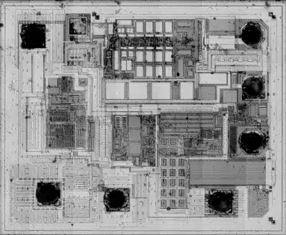
As MEMS devices become smaller and more complex, conventional wafer maps are no longer sufficient for detailed defect analysis and process optimization. Traditional wafer maps categorize dies at a high level (e.g., “pass,” “fail,” or specific defect categories), but they lack the granularity to pinpoint the exact nature and location of defects within a die. This limitation is especially problematic as modern MEMS architectures integrate multiple functionalities and shrinking dimensions make even minor defects impactful.
Automated Optical Inspection (AOI) systems may capture pixel-level defect data, but without integrating this information into wafer maps, manufacturers struggle to localize defects and correlate issues with specific process steps. This hampers targeted process improvements and increases defect escape rates, leading to higher costs and potential reliability issues.
Advanced bin wafer map capabilities that integrate AOI data are essential for modern MEMS manufacturing. These tools perform atomic-scale analysis, address the challenges of increasing device complexity, and ensure improved yields.
3. Scale of Operation
MEMS devices are highly intricate, with each pixel in the sub-circuitry representing a potential site for defects or performance variations. Traditional testing methods struggle to capture and localize these micro-scale issues, particularly when voltage irregularities occur that are too subtle or localized for high-level inspection tools to detect.
This lack of granularity hampers effective issue diagnosis. It also risks allowing defective devices to progress through production, impacting both yield and reliability. The challenge is further amplified by the need to process vast amounts of data generated during testing, requiring advanced yield management tools, like yieldWerx, to extract actionable insights from these complex datasets.
4. Integrating Wafer-Level and Package-Level Testing for MEMS Yield Optimization and Reliability
Wafer-level electrical testing is essential for assessing MEMS sensor yield, allowing for early defect isolation. However, predicting package-level yield based solely on wafer-level tests is challenging due to packaging-induced variables, even though advancements have improved their accuracy significantly.
Reliability assessments at the package level often focus on hermetic sealing to protect MEMS devices from environmental factors, ensuring long-term performance and reliability. This combination of wafer-level and package-level testing ensures high-quality MEMS devices with optimized yields and robust functionality.
MEMS yield modelling is an evolving field that adapts techniques from IC design to address the unique complexities of MEMS device fabrication. Accurate yield modeling relies on comprehensive defect data, grouped by failure mechanisms or fault classes rather than critical area methods. Key methodologies include Monte Carlo simulations for predicting the impact of process variations and functional yield modelling to optimize MEMS design and enhance reliability before fabrication.
4. Testing Frequency
The challenge lies in balancing rigorous testing to ensure MEMS device reliability without causing damage to sensitive components. Overtesting can degrade delicate structures, such as thin membranes or movable parts, through excessive mechanical, thermal, or electrical stress. Conversely, undertesting can risk missing subtle issues like bias temperature instability (BTI), leading to premature failures in critical applications like the automotive industry where testing requirements are higher.
This balance becomes even more complex at high production volumes, where testing must simulate operational and environmental conditions efficiently without introducing defects. Sophisticated test methods and yield management software are essential to achieve comprehensive yet non-destructive testing.
Managing MEMS Yield and Reliability with yieldWerx
yieldWerx addresses the lack of standardization in MEMS manufacturing by offering adaptable solutions that bridge the variability inherent in MEMS fabrication processes. Its powerful modules process non-standard data logs, including pixel/bitmap data in proprietary formats, helping you deal with the challenges posed by the absence of universal MEMS testing standards. You don’t have to manually dig through individual logs any more.
Custom parsers developed by our team of engineers ingest diverse datasets, allowing test houses and fabless companies to analyze data without relying on specialized tools, regardless of the format or device vendor.
When it comes to overcoming the limitations of traditional wafer maps, yieldWerx assists MEMS engineers by combining pixel-level Automated Optical Inspection (AOI) data into bin wafer maps. Users can render and analyze granular defect data for each die. This provides a detailed view of the exact nature of defects within a MEMS sub-circuitry resulting in better yields and device reliability.
yieldWerx also addresses the challenges of atomic-scale defect detection in MEMS devices through parametric heat map analysis at the pixel or bitmap level. This capability allows manufacturers to visualize peak-to-peak voltage variations across all locations within the MEMS sub-circuitry, providing the granularity needed to identify subtle irregularities that traditional testing methods often miss. By capturing and localizing these voltage deviations, yieldWerx ensures that potential defects are diagnosed effectively before they progress through production.
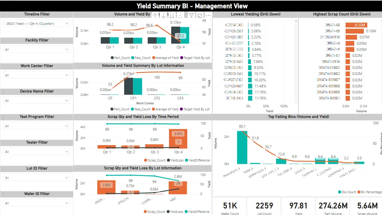
Lastly, we provide customizable BI dashboards that display comprehensive analyses for each MEMS die across pixel data and identify critical defects data. They can fully monitor specific test indices such as normalized heat maps with corresponding signal amplification and noise suppression capabilities of a unit. By combining detailed pixel data with high-level parametric insights, yieldWerx’s BI dashboards provide a centralized and actionable view of MEMS yield performance.
Are you struggling to manage MEMS test data logs? See yieldWerx in Action – Schedule a Demo Today!
FAQs
What are the Substitute Terminologies for MEMS?
Companies with Japanese origins refer to them as micromachines, while those based in Europe call them microsystem technologies.
What is Pixel Defect Data?
Pixel or bitmap data is graphical information representing images in a grid of pixels (e.g., for visual inspection or image processing tasks).
What are Pixel Defects in MEMS sub-circuitry?
Pixel defects in a MEMS sub-circuitry refer to localized anomalies or imperfections in the individual components of the MEMS device’s functional structure. These defects can arise in the electrical, mechanical, or optical aspects of the device, depending on its design and purpose. For example, a single micromirror stuck in the “on” or “off” position results in a bright or dark spot in projected images.
What is Data Parsing?
Data parsing is the process of extracting relevant information from unstructured data sources and transforming it into a structured format that can be easily analyzed. A data parser is a software program or tool used to automate this process.
What is a Heat Map?
A heat map visually represents data values as colors, often used to highlight parametric variations or patterns across a spatial layout.
What is Peak-to-Peak Voltage?
Peak-to-peak voltage is the total voltage difference between the maximum positive and negative peaks of a waveform.

