AI-Powered PAT: A New Era of Smarter Manufacturing
For the past three decades, the Automotive Electronics Council (AEC) has utilized Part Average Testing (PAT) as the standard for statistical screening. However, technological advancements beyond Moore’s Law have outpaced the capabilities of traditional PAT methods.
PAT typically uses univariate statistical methods—comparing each test parameter to a limit derived from the population mean and standard deviation. While this approach was practical in earlier manufacturing nodes, it struggles to account for the complex, multi-dimensional interactions now present in modern chip design.
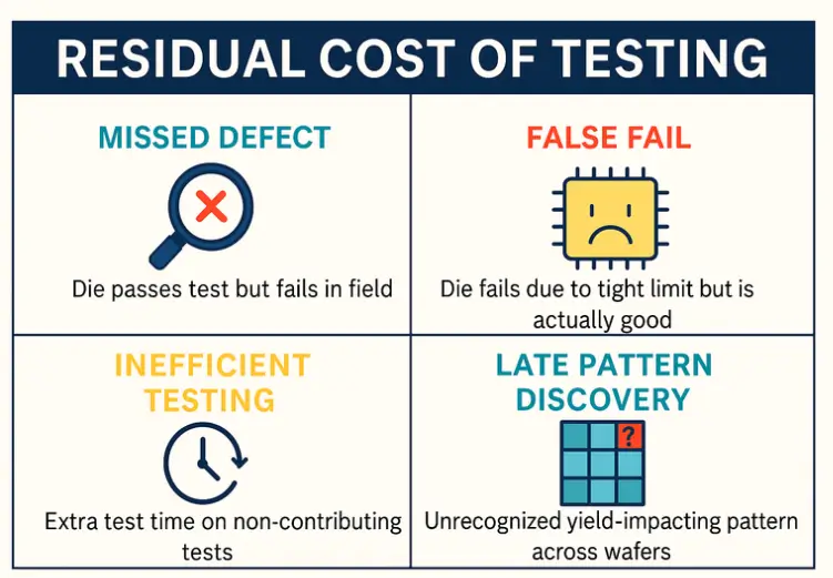
Today’s devices undergo thousands of electrical tests, but not all defects are captured by individual test thresholds. Subtle process variations, spatial anomalies, and early indicators of degradation often fall through the cracks. Dies that pass all standard limits may still harbor latent defects that result in customer quality incidents (CQIs). At the same time, overly tight or static PAT limits can lead to false positives, causing the scrapping of otherwise good dies and unnecessarily reducing yield. Smart manufacturing relies on smart testing. Efficiency can be improved by scaling back tests that don’t strongly correlate with CQI data, thereby creating a balance of quality and yield based on the criticality of different applications.
Another major challenge is that conventional PAT assumes normal distributions and fixed test behavior across lots and products. This assumption breaks down in high-mix, high-complexity environments. Advanced PAT methods, such as Dynamic PAT (DPAT) or Robust PAT (RPAT), are just a few of the enhancements that have evolved from traditional PAT with modifications to correct skewness and distributions, improving efficiency. Traditional outlier detection approaches may fail to account for the rich, heterogeneous data generated across the manufacturing flow—such as spatial coordinates, inline inspection data, or cross-wafer trends.
As a result, semiconductor companies are increasingly adopting machine learning (ML) to enhance traditional PAT and perform multivariate analysis that can detect patterns invisible to legacy methods. AI and ML models can learn from historical data to uncover subtle relationships across multiple parameters, adapt to product-specific behaviors, predict failure patterns, and lower residual testing costs.
Balancing Performance and Reliability with CQIs
The truth is, some electrical measurements are more closely related to latent defects than others; thus, not all outliers have an equal impact. For those tests that have a lower correlation to latent defects, less rigorous testing can be adopted to improve yield. CQI’s provide a method to identify the tests that have a high correlation to latent defects. Over time, each prevented CQI compounds the savings by reducing customer dissatisfaction, logistics costs, and engineering hours spent on failure analysis. That’s why even small optimizations in PAT thresholds, test selection, or spatial filters—when scaled across millions of units—can yield massive financial and operational benefits.
Balancing Test Sensitivity and Yield Loss in Outlier Detection
Statistical algorithms like advanced PAT and outlier detection save significant time by automating the identification of at-risk dies, but they come with important tradeoffs—particularly when calibrating them based on CQI data.
The main challenge lies in balancing sensitivity and yield loss. If the screening criteria are too aggressive (e.g., tight limits or broad bin exclusions), the algorithm may catch more potential CQIs but at the cost of discarding too many good dies, resulting in unnecessary yield loss. Conversely, if the screening is too lenient, latent defects may slip through, leading to costly customer returns.
Setting up CQI-based outlier detection requires historical failure analysis, correlation of test bins with known CQIs, and careful parameter tuning—steps that add initial complexity and effort. However, once calibrated properly, these models enable targeted, high-confidence screening, significantly reducing false positives and missed defects.
For chip makers, the benefit is twofold:
- Improved quality at the source—fewer escapes mean fewer field failures and better customer trust.
- Cost savings at scale—even a small drop in CQIs across millions of units results in substantial reductions in warranty claims, rework, and engineering support costs.
In short, the tradeoff is complexity upfront, but the long-term gain is controlled yield loss with maximum CQI impact, making the investment highly worthwhile.
ML and AI Can Supercharge Geo-Spatial Pattern Recognition
Today, detecting CQI-related patterns—especially spatial or parametric outliers—is often done manually by engineers through a combination of visual inspection, rule-based filters, and historical data review. This typically involves:
- Manually inspecting wafer maps to look for clusters or anomalies (e.g., edge failures, hot spots).
- Comparing test parameters against known thresholds or limits.
- Running scripts to correlate failed bins with past CQIs.
- Relying on experience to interpret patterns that might signal latent defects.
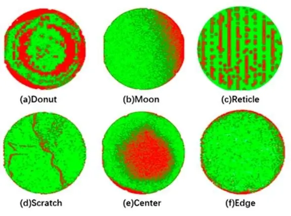
This manual process is time-consuming, often taking days or weeks, especially when dealing with thousands of wafers and millions of dies. It also leaves room for human bias and inconsistency, and subtle patterns—like corner-case fails or evolving process drifts—can easily be missed.
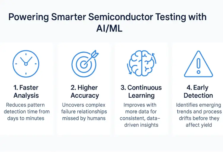
By using AI/ML, the process becomes faster, more scalable, and more accurate:
- Time savings: Pattern recognition that takes days manually can be done in minutes or seconds using trained models.
- Higher accuracy: ML models can uncover non-obvious relationships between test data, spatial layout, and CQI history—patterns humans may overlook.
- Continuous learning: These models improve over time with more data, refining detection capabilities with every lot processed.
Machine learning (ML) and artificial intelligence (AI) can significantly improve the identification of geospatial patterns in DPAT, AECPAT, and GDBN by moving beyond rule-based methods leading to less false-positives (overkills). Traditional approaches often miss complex or subtle relationships between die failures, especially when those failures occur in specific regions or follow unique spatial trends.
ML and AI can analyze vast amounts of test and location data across wafers to recognize patterns that aren’t obvious to human engineers or basic statistical methods. For example, if certain regions of a wafer consistently show higher failure rates—even if the individual dies appear to pass conventional tests—AI can highlight those areas as potentially problematic.
In the case of GDBN, AI can enhance the understanding of how a failed die might affect its surrounding neighbors by learning from historical data rather than relying solely on fixed proximity rules. Over time, these systems can even anticipate emerging issues by spotting changes in spatial behavior across wafers or lots. This is useful not just for the automotive industry but also consumer and medical electronics.
Edge Prediction
Edge Prediction refers to the application of machine learning directly at production and assembly facilities, enabling localized decision-making based on real-time test data. This approach requires reliable mechanisms to deploy and update models, access compute infrastructure on-site, and potentially integrate with factory automation and control systems.
One key application is die grading and exclusion, where ML is used to evaluate individual die performance against test populations. Another important use case involves the computation of die quality metrics, where data from lot equipment history, parametric tests, visual inspections, and electrical tests are used to infer the quality of each die and recommend whether further testing is needed or can be avoided.
Deployment Challenges with ML systems
Integrating AI/ML into semiconductor testing presents several challenges. Data collection is a critical hurdle, as AI models depend on comprehensive data to function accurately. Semiconductor manufacturing also involves diverse data types from different sources, such as equipment metrics and wafer inspection results, which must be integrated into the production flow.
However, issues like siloed data, compatibility between equipment, and ensuring sensor accuracy complicate the process. AI’s success depends on high-quality, real-world measurement data rather than relying too much on simulation data, which can overlook crucial factors.
Furthermore, the constant evolution of processes requires that AI models be frequently updated to reflect new baselines. To effectively implement AI/ML, fabs and test houses need to collect vast amounts of data while ensuring traceability.
Basic algorithms might not pose a security risk, but more advanced machine learning models can be sensitive. Some platforms, like C-language models, are harder to reverse-engineer, while others, like Python, are more transparent. For companies concerned with security, strong encryption, obfuscation, or server-side security measures may be necessary.
By using a combination of dimensionality reduction, non-parametric models, multivariate analysis, and continuous learning, semiconductor manufacturers can optimize testing processes, reduce defects, and lower costs while maintaining high product quality.
- Data Dimensionality – With thousands of electrical tests and parameters, determining which tests are most relevant for quality screening is difficult.
- Non-Normal Distributions – Traditional outlier detection techniques assume Gaussian (normal) distributions, which may not hold in real-world semiconductor data, making it challenging to detect anomalies accurately.
- Multivariate Nature – Device quality often depends on interactions between multiple test parameters, not just individual tests. Capturing these complex relationships is a challenge for traditional methods.
- Insufficient Training Data – In some cases, there isn’t enough labeled data for all failure types, particularly for rare or field-related failures, making accurate predictions challenging.
- Scalability and Computational Complexity – Implementing ML models and maintaining their performance across millions of units can be computationally intensive, especially in real-time testing scenarios.
- Feature Selection – Choosing the most predictive features (test parameters) for accurate ML model performance can be a challenging and time-consuming process.
yieldWerx Powers the Future of Part Average Testing
Staying ahead of these advancements, yieldWerx’s AI/ML capabilities continue to shape the future of Part Average Testing (PAT) by continuously improving our proprietary outlier detection algorithms, including Zonal PAT and PAT++. Our powerful Quality Control & Risk Containment module helps integrate large and complex test datasets, leveraging advanced machine learning to identify and predict outliers as we assist our customers in achieving zero defects.
Contact Us to learn more about our different PAT solutions.
Learn how yieldWerx’s AI/ML capabilities for Part Average Testing help companies detect outliers, reduce latent defects and semiconductor maximize yields.


