
Wafer map calculators are important for semiconductor manufacturing, playing a key role in optimizing production outcomes and improving yield. These calculators facilitate the gross die per wafer calculation, yield improvement, and production optimization by providing detailed insights into the wafer surface and identifying patterns that could indicate potential issues.
Their importance in the semiconductor industry is significant due to their contribution to improving production efficiency and implementing strategies for yield improvement. By aiding in defect data management and quality control, these calculators are indispensable for maintaining the competitiveness of the semiconductor industry, making them key for production optimization and effective yield management.
Understanding Wafer Map
Source: Advanced Software Engineering Ltd
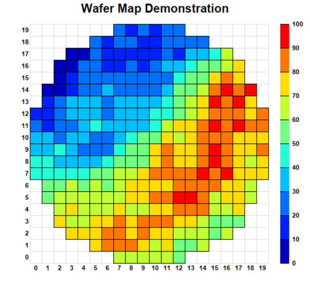
Wafer maps are graphical representations that detail the defects found on semiconductor wafers during the manufacturing process. These maps are generated using wafer map calculators, employing statistical analysis and visualization tools to depict defect locations and densities on the wafer surface accurately.
This technology plays a pivotal role in semiconductor yield management by allowing for a comprehensive examination of the patterns that defects form on the wafer, facilitating a deeper understanding of the production process.
Significance in Quality Control and Yield Improvement
The importance of wafer maps in quality control and yield improvement cannot be overstated. Through detailed wafer defect analysis, these maps provide essential insights into the manufacturing process, highlighting areas that require attention.
This, in turn, supports the implementation of yield enhancement strategies and semiconductor production efficiency by identifying and addressing the root causes of defects. As a result, wafer maps are integral to maintaining high standards of quality control and driving continuous improvement in semiconductor manufacturing.
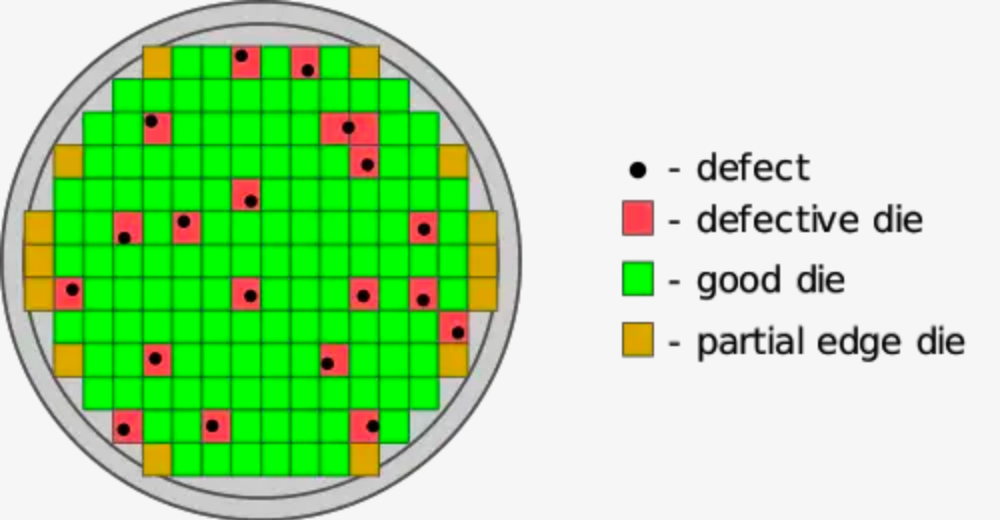
Key Elements in a Wafer Map
A wafer map includes several key elements that are critical for defect identification and analysis. These elements include the type of defects, their location on the wafer, and the density of defects across the wafer surface.
By utilizing data visualization in manufacturing, wafer maps make it easier for engineers to interpret complex data, enabling the effective management of defect data and the application of statistical process control.
Moreover, monitoring tools integrated with wafer map calculators improve the ability to track and respond to issues promptly, further optimizing the production process in the semiconductor industry.
The Role of Wafer Map Calculators
The role of wafer map calculators in data analysis is vital. They apply statistical analysis to identify patterns on semiconductor wafers, making complex data more accessible and actionable.
Contribution to Data Analysis
Wafer map calculators are key in transforming the complex data associated with semiconductor wafers into actionable insights.
Through advanced statistical analysis and the use of sophisticated visualization tools, these calculators allow for a detailed examination of the wafer surface, uncovering patterns that might not be visible to the naked eye.
This capability is vital for defect identification, enabling semiconductor industries to conduct thorough wafer defect analysis. By analyzing the data generated, engineers can pinpoint specific areas of concern on the wafer, facilitating targeted interventions to address these issues.
Importance in Optimizing Production Processes
The optimization of production processes in semiconductors heavily relies on the insights provided by wafer map calculators. These tools play a key role in semiconductor yield management by offering a granular view of yield-related data, which is essential for gross die per wafer calculation and yield improvement efforts.
By identifying defect patterns and trends, wafer map calculators aid in the formulation of yield enhancement strategies and ensure semiconductor production efficiency. This not only leads to a reduction in waste but also contributes to higher-quality outputs.
Key Features of Wafer Map Calculators
Wafer map calculators stand at the forefront of technological innovation in the semiconductor industry, equipped with features designed to address the complex challenges of semiconductor manufacturing. These tools are not just about data analysis; they are about transforming data into a strategic asset for yield improvement, quality control, and operational efficiency.
Statistical Analysis Capabilities
Wafer map calculators are equipped to process complex datasets, identifying patterns and irregularities on wafer surfaces that could negatively affect yield. This capability is vital for thorough wafer defect analysis and ensuring quality control, helping users make decisions that improve yield.
Visualization Tools for Easy Interpretation
These calculators include visualization tools that convert complex statistical data into user-friendly formats, such as charts and graphs. This feature simplifies identifying problem areas on the wafer, making the defect identification process more efficient. It greatly aids in managing semiconductor yield by making data easier to understand and act upon.
Integration with Other Semiconductor Tools
An important feature of wafer map calculators is their ability to work cohesively with other semiconductor manufacturing tools.
Such integration is key to effective defect data management, consistent quality control, and the successful implementation of yield improvement strategies.
Applications in the Semiconductor Industry
Source – https://en.wikichip.org/wiki/yield
Wafer map calculators underpin critical aspects of semiconductor manufacturing, from improving quality control to driving yield improvements. Their use in defect analysis and yield management strategies is integral to advancing semiconductor production efficiency, ensuring the industry continues to meet the escalating demands for high-quality, reliable semiconductor devices.
Quality Control in Manufacturing
Wafer map calculators are essential for ensuring quality control in the semiconductor manufacturing process. Using gross die-per-wafer calculation, these tools assess the viability of semiconductor wafers, identifying defects on wafer surfaces through statistical analysis and visualization techniques.
This careful examination ensures that only wafers meeting high-quality standards continue through the production line, maintaining the semiconductor industry’s high reliability and performance.
Yield Improvement Strategies
These calculators are also important in formulating and applying strategies to increase yield. They analyze semiconductor wafers to identify patterns and defects that could affect yield, aiding in semiconductor yield management. The insights provided by wafer map generation and defect analysis allow manufacturers to adjust their processes to reduce waste and boost the efficiency of semiconductor production, thereby maximizing output.
Defect Identification and Analysis
Identifying and analyzing defects accurately is a critical capability in semiconductor manufacturing, made possible by wafer map calculators. They offer an in-depth look at wafer defect patterns, facilitating accurate defect identification.
Through detailed wafer defect analysis and the application of statistical process control, manufacturers can identify the causes of defects that impact yield and take corrective action. This precise analysis aids in effective defect data management and quality control, ensuring semiconductor products meet the industry’s strict standards.
Advantages of Using Wafer Map Calculators
Here are the advantages of using wafer map calculators in the semiconductor manufacturing process:
Time Efficiency in Data Analysis
Wafer map calculators offer a significant reduction in the time needed for data analysis within semiconductor manufacturing. They automate complex calculations, such as gross die per wafer, and apply detailed statistical analysis, facilitating quicker decision-making in yield management.
This speed is essential for the rapid generation of wafer maps and the analysis of defects, contributing to the overall efficiency of semiconductor production processes.
Enhanced Accuracy in Identifying Patterns
These calculators improve the precision of identifying defect patterns on semiconductor wafers. Equipped with advanced visualization tools, they deliver detailed mappings of wafer surfaces, exposing patterns that might otherwise remain hidden.
This precision is essential for accurate defect identification and for ensuring the effectiveness of quality control measures, leading to more efficient manufacturing processes and improved yield outcomes.
Real-time Monitoring Capabilities
Equipped with monitoring tools, wafer map calculators allow for the ongoing observation of manufacturing processes.
This feature is essential in identifying and addressing issues as they arise, ensuring quick action can be taken to manage defects effectively. Monitoring the production environment in real-time is vital for upholding high-quality standards in semiconductor manufacturing, ensuring quick responses to maintain efficiency and product quality.
Choosing the Right Wafer Map Calculator
Choosing an effective wafer map calculator is important for semiconductor manufacturing efficiency and yieldWerx provides an exceptional solution. It specializes in delivering detailed wafer map calculations and generation, offering capabilities for gross die per wafer calculation and extensive statistical analysis, which are essential for yield improvement. The platform’s visualization tools transform complex data on wafer surfaces into understandable visual formats, significantly aiding defect identification and quality control efforts.
yieldWerx also features monitoring and integrates smoothly with existing semiconductor production processes, adding significant value to yield management and production optimization. Efficient wafer map generation and precise defect analysis assist in maintaining production efficiency and formulating effective yield enhancement strategies. As a result, yieldWerx becomes an indispensable tool for semiconductor manufacturers focused on refining their production processes and achieving superior yield outcomes efficiently.
Trends in Wafer Map Calculators
The field of wafer map calculators is undergoing rapid changes, with new technologies and innovations shaping the future of semiconductor manufacturing. These developments are pushing the boundaries of what’s possible in wafer map analysis, offering improved methods for semiconductor yield management and production efficiency.
Integrating machine learning and artificial intelligence (AI) into wafer map calculators marks a significant shift towards more sophisticated wafer defect analysis. AI can uncover subtle defect patterns on semiconductor wafers, advancing defect identification and quality control. This move towards smarter analysis tools reflects a larger trend towards data-driven decision-making in manufacturing, where complex data insights guide operational strategies.
Advancements in data visualization are simplifying the interpretation of wafer map data, allowing engineers to make quicker, informed decisions. When combined with monitoring capabilities, these tools permit on-the-fly adjustments to the manufacturing process, thus optimizing production efficiency.
Case Study
Automated Wafer Map Failure Pattern Classification
A study from Stanford University demonstrates the use of deep learning convolutional neural networks (CNNs) to automate wafer map failure pattern classification. The project used the WM-811K (LSWMD) dataset from Kaggle, which consists of 811,457 wafer maps. Researchers developed and optimized models to improve the accuracy and efficiency of analyzing large-scale wafer map datasets.
Accurately identifying defect patterns in wafer maps can help engineers find abnormal failure factors in production lines, leading to improved product quality and reduced costs.
Foreword
Wafer map calculators are essential in semiconductor manufacturing, providing detailed analysis of wafer defects and aiding in developing strategies for improved yield. These tools use statistical methods and visual representations to identify production issues and optimize operations.
yieldWerx™ is recognized as a significant tool, offering strong capabilities for defect analysis and yield management, becoming an important asset in the semiconductor sector.
Frequently Asked Questions (FAQs)
1- What is a wafer map calculator, and how does it differ from other semiconductor tools?
A wafer map calculator specializes in analyzing defects on wafer surfaces and calculating the gross die per wafer, setting it apart from other tools by offering a blend of statistical analysis and visualization capabilities. This tool is integral for detailed defect management and yield calculation, unlike others focusing on specific production stages.
2- How do wafer map calculators contribute to the improvement of semiconductor yield?
By providing detailed defect analysis and identifying patterns on semiconductor wafers, wafer map calculators support yield improvement. They apply statistical process control and develop strategies for yield enhancement, thus directly contributing to semiconductor production efficiency.
3- Are there any specific industries or applications outside semiconductor manufacturing where wafer map calculators can be useful?
Beyond semiconductor manufacturing, wafer map calculators find applications in industries like photovoltaic cell production and MEMS, where surface analysis and defect management are critical for optimizing yield and production processes.
4- What challenges are commonly associated with wafer map analysis, and how can they be addressed?
Challenges include managing large datasets and identifying defect patterns accurately. Solutions involve advanced visualization tools and real-time monitoring, which help break down complex data and facilitate prompt defect identification.
5- Is it necessary for semiconductor companies to invest in expensive wafer map calculator software, or are there cost-effective alternatives available?
Not all semiconductor companies need to invest in high-cost software. Cost-effective alternatives provide key features for wafer map generation and basic analysis, suitable for yield management and defect analysis needs.
6- How do wafer map calculators handle large datasets, and what strategies exist for efficient data analysis?
To manage large datasets, wafer map calculators use advanced algorithms and visualization tools. Efficient data analysis strategies include data segmentation and real-time feedback to adjust analysis techniques continuously.
7- Are there any regulatory considerations or standards for using wafer map calculators in semiconductor manufacturing?
While specific regulations for wafer map calculators may not exist, semiconductor manufacturing must adhere to industry standards that ensure quality and efficiency. These tools support adherence by facilitating accurate defect analysis and effective yield management.
8- How can companies maximize the benefits of wafer map calculators in their production processes?
Companies can maximize the benefits by integrating these calculators throughout production for comprehensive defect analysis and yield management. Training teams to use these tools effectively and to understand the data they produce can significantly improve production outcomes.


