
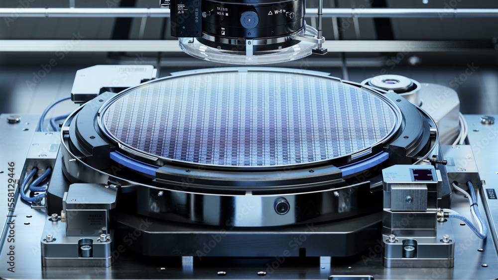
Why is Semiconductor Wafer Inspection Important?
Wafer inspection is one of the most remarkable steps in the production of semiconductor devices, as it verifies the accuracy and functionality of the wafers, which serve as the basis for all semiconductor devices.
This article explores the many reasons that wafer inspection is vital for semiconductors.
The Role of Wafer Inspection in Key Manufacturing Stages
Photolithography
This process involves transferring a pattern onto the wafer. Wafer inspection here verifies that the patterns are accurately imprinted without any misalignments or defects, which could otherwise lead to circuit failures.
Etching
Etching removes layers from the silicon wafer to create the intended circuit patterns. Wafer inspection at this stage checks for uniformity and precision in the etched patterns, identifying any irregularities that might impact the performance of the final device.
Doping
Doping alters the electrical properties of the silicon wafer. Wafer inspection after doping is important to confirm that the desired electrical characteristics have been achieved uniformly across the wafer.
Layer Deposition
Various layers are deposited on the wafer to form the electronic circuits. Wafer inspection verifies that all layers are appropriately deposited and free of defects such as contaminants or uneven thickness.
Final Inspection
Following completion processing, a final wafer inspection is carried out to make sure the finished wafers adhere to all necessary criteria. This includes examining the product’s general quality, electrical function, and physical defects.
Achieving Semiconductor Integrity with Wafer Inspection
Wafer inspection assures semiconductor quality control by carefully examining each wafer to identify and address any flaws that could impact device performance and maintain high standards of precision and accuracy.
The Scope of Wafer Inspection
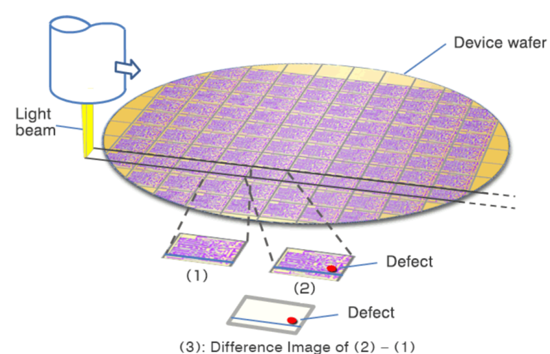
Detection of Microscopic Defects
Wafer inspection detects the slightest imperfections, including tiny particles, minute scratches, or unwanted pattern deviations. These defects, although microscopic, can lead to major issues in the functionality of devices.
For instance, Scanning electron microscopes (SEMs) are used in wafer inspection to detect microscopic defects. By scanning a focused electron beam across the wafer and capturing emitted secondary electrons, SEMs produce high-resolution images that can identify defects as small as a few nanometers.
Pattern Accuracy
Modern semiconductor devices are built with incredibly complex patterns. Wafer inspection warrants that these patterns are accurately replicated on the wafers, without any deviations. Even the slightest error in patterning can lead to a cascade of problems in electronic circuits.
Surface Analysis
The inspection also involves a thorough analysis of the wafer surface. Any irregularities on the surface can impact the subsequent manufacturing processes, such as lithography or layer deposition.
Precision in Wafer Inspection
The process employs advanced technologies such as high-resolution imaging, laser scanning, and sophisticated software algorithms to detect and analyze defects. The aim is to identify issues at the earliest possible stage to prevent them from escalating into considerable problems in the final product.
The Impact of Flaws Detected in Wafer Inspection
The smallest flaw detected during wafer inspection can have far-reaching effects. This is particularly important in applications where reliability is paramount, such as medical devices, automotive systems, or communication infrastructure. Thus, wafer inspection is a quality control measure and an essential safeguard against potential failures.
Cost Savings through Early Defect Detection
Early defect detection during wafer inspection is vital in preventing costly errors in the later stages of the manufacturing process, and optimizing processes through wafer inspection increases both yield and efficiency.
Early Defect Detection and Its Economic Advantages
Preventing the Progression of Defects
Identifying defects at the wafer inspection stage prevents these defects from progressing through the subsequent, more expensive stages of production. Detecting and addressing defects early on saves substantial costs that would otherwise be incurred in later stages.
Minimizing Rework and Scrap
Wafer inspection significantly reduces the need to rework or scrap wafers. Reworking a wafer or, worse, scrapping it after several processing stages have been completed is considerably more costly than identifying and addressing a defect during an initial step.
Reducing Downstream Impacts
Flaws that go unnoticed during wafer inspection can lead to failures in the final semiconductor product. These failures can have downstream impacts, such as recalls, warranty claims, and damage to brand reputation, all of which entail high costs.
Optimizing Processes
Boosting Yield
Improvements based on wafer inspection findings can lead to increased yield, meaning a higher percentage of wafers meet quality standards, thereby increasing the output efficiency.
Process Improvement and Efficiency
Wafer inspection data provides insights that can be used to improve manufacturing processes. Manufacturers can improve their operations by understanding and addressing the root causes of defects identified during wafer inspection, leading to more efficient production and reduced waste.
Feedback Loop for Continuous Improvement
Regular and detailed wafer inspection creates a feedback loop for continuous improvement. By consistently monitoring and analyzing the wafer inspection results, informed decisions can be made that lead to ongoing process refinement and cost reduction.
Compliance
Wafer inspection confirms that the products are reliable, safe, and perform to expectations. Regular and rigorous checks are critical to maintaining compliance in the highly regulated semiconductor industry.
Adherence to Industry Standards
Quality Standards
Wafer inspection verifies that the wafers meet specific quality standards that often include criteria for material purity, pattern accuracy, and defect levels. Manufacturers can certify that their products consistently meet these established quality benchmarks.
In wafer inspection, quality standards commonly include:
- Material Purity: Standards such as ASTM F123 (Standard Specification for Semiconductor Grade Silicon) specify the acceptable levels of impurities in the silicon used to produce wafers.
- Pattern Accuracy: This involves ensuring that the circuit patterns etched onto the wafers are precise down to the nanometer. Deviations from specified geometries can lead to non-functional or inefficient chips.
- Defect Levels: Standards like the ITRS (International Technology Roadmap for Semiconductors) define the maximum number of defects per square centimeter that are permissible. These defects could be particles, scratches, or unwanted pattern deviations.
Safety and Reliability
Wafer inspection helps to confirm that the chips used in applications like automotive systems and aerospace technology are high in quality, safe, and reliable for their intended uses.
Regulatory Compliance
The semiconductor industry is subject to various regulatory requirements, which may vary depending on the region and application. Wafer inspection makes sure of compliance with these regulatory standards, thus avoiding potential legal and financial repercussions.
A few key regulations include:
- ISO 9001: This international standard dictates quality management systems and is essential for manufacturers to demonstrate their ability to consistently produce quality products.
- REACH and RoHS in the European Union: These regulations restrict hazardous substances in electrical and electronic equipment and require manufacturers to manage the risks associated with chemical use.
- SEMI Standards: Developed by the global industry association SEMI, these standards cover everything from equipment interfaces to the specifications for materials used in chip manufacturing, including guidelines for wafer surface quality.
Importance of Meeting Quality and Reliability Requirements
High-Quality Products
The semiconductor industry demands high-quality products, given the critical nature of their applications in various fields. A high level of quality is maintained by verifying that every wafer, and thus every chip, is free from defects that could impair their performance.
Reliability and Long-Term Performance in Various Applications
Wafer inspection is essential for ensuring that semiconductor devices are reliable and perform consistently across various applications. The quality control processes employed during manufacturing, such as thorough wafer checks, are fundamental to guaranteeing that the wafers are defect-free and meet all specifications. This attention to detail ensures that the final products are less likely to fail, providing reliable safety and sustained performance over time.
Customer Confidence and Market Reputation
Meeting quality standards builds customer confidence and increases the manufacturer’s reputation in the market. Adherence to quality standards is key to long-term success and customer loyalty.
Avoiding Costly Recalls and Repairs
Effective wafer inspection reduces the likelihood of product failures that could lead to costly recalls and repairs. Making sure that products are compliant and reliable from the outset saves manufacturers from potential financial and reputational damages associated with product failures.
yieldWerx: Improving Wafer Inspection Processes
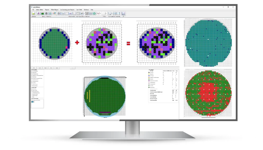
Processing test data, inspection data, and manufacturing operating procedures are required when moving from a wafer to a set of packaged units.
Engineers and operators can use the wafer map generation module to build the wafer map needed for inspection processes and assembly facilities when combined with other yieldWerx modules.
yieldWerx increases the efficiency and accuracy of defect identification, playing an important role in the continuous improvement of semiconductor product yield and reliability.
Conclusion
Wafer inspection is a fundamental aspect of the semiconductor manufacturing process, vitally important for ensuring product quality, improving cost efficiency, and maintaining compliance with industry standards. As technological advancements continue, the role of wafer inspection becomes increasingly vital in producing reliable, high-quality semiconductors.
It not only helps in early defect detection, reducing potential costs, but also contributes to process optimization and higher yield rates. In an industry where precision is paramount, wafer inspection remains a significant practice for meeting the growing demands and complexities of semiconductor device manufacturing.
Frequently Asked Questions (FAQs)
1. What technologies are used in semiconductor wafer inspection?
Semiconductor wafer inspection often uses advanced technologies like high-resolution microscopy, automated defect classification systems, and machine learning algorithms to detect and analyze defects on wafers.
2. How often is wafer inspection performed during manufacturing?
Wafer inspection is typically performed at multiple stages throughout the semiconductor manufacturing process, especially after critical steps like photolithography, etching, and doping, to ensure continuous quality control.
3. What is the impact of wafer inspection on semiconductor device reliability?
Wafer inspection significantly impacts device reliability by identifying potential defects that could lead to device failure, making sure only high-quality wafers are used in the production of semiconductor devices.
4. Is wafer inspection automated or manual?
Wafer inspection incorporates both automated and manual methods. Automated inspection is faster and more consistent for standard defect identification, while manual inspection is used for more complex analysis.
5. What happens to wafers that fail inspection?
Wafers that fail inspection are typically either reworked, if possible, to correct the defects or discarded to prevent defective end products, depending on the nature and severity of the defects detected.
6. How does wafer inspection contribute to environmental sustainability in manufacturing?
By identifying defects early and reducing waste, wafer inspection contributes to more sustainable manufacturing practices, as it minimizes the resources and energy used to produce semiconductor devices.

