Zero Defect Tools in the Semiconductor Industry
The semiconductor industry is highly advanced and constantly evolving, with manufacturers always seeking new ways to improve their processes and reduce defects. There are several tools and techniques that are commonly used in the industry to achieve, zero defects or near-zero defect rates.
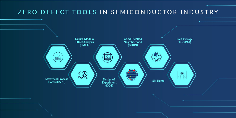
Here are some of the most commonly used tools:
Statistical Process Control (SPC):
This is a data-driven method that monitors and controls the production process by collecting and analyzing data in real-time. SPC semiconductor can identify when a process is deviating from its normal behavior, allowing engineers to take corrective action before a defect occurs.
Failure Mode and Effects Analysis (FMEA):
This is a method used to identify potential failure modes and their impact on the product, process, or system. FMEA is often used in the early stages of product design to identify potential issues and take corrective action before the product goes into production.
Design of Experiments (DOE):
This is a method used to systematically test and analyze the effects of various factors on a process or product. DOE can identify the optimal settings for process parameters and help to minimize variation in the production process.
Good Die/Bad Neighborhood (GDBN):
This is a tool that analyzes data from semiconductor wafer test results to identify patterns that can indicate issues with the manufacturing process. By identifying “neighborhoods” of dies that are experiencing high levels of failure, engineers can quickly isolate the source of the issue and take corrective action.
Six Sigma:
This is a methodology used to systematically reduce defects and variation in a process or product. Six Sigma uses a data-driven approach to identify and eliminate the root causes of defects, with the goal of achieving a defect rate of less than 3.4 defects per million opportunities.
Part Average Test (PAT):
Part Average Test evaluates the performance of individual components within an integrated circuit (IC). It detects and removes outliers by statistically analyzing a sample of parts and excluding those with performance outside of a predetermined range from the average performance calculation.
These tools are just a few examples of the many techniques that are used in the semiconductor industry to achieve zero defects or near-zero defect rates. By using these tools and constantly striving to improve their processes, manufacturers can ensure that their products are of the highest quality and reliability, meeting the demanding standards of their customers. yieldWerx provides all these tools and techniques in their yieldWerx Enterprise solution for semiconductor industry.
You can explore the benefits of “yieldWerx Enterprise” modules in terms of improving production and achieving zero defects also speeding up product launch by signing up for a 15-Day Free Trial and Scheduling a Live Demo.


