Gross die yield, a critical metric in semiconductor manufacturing, reflects the proportion of functional chips produced from a wafer. It’s a key indicator of manufacturing efficiency, influencing the cost and quality of semiconductor products. High gross die yield guarantees optimal use of materials. It improves product quality, making it essential for manufacturers to prioritize yield optimization, defect management, and wafer yield management to stay competitive.
Maximizing gross die yield is vital for cost-effectiveness and maintaining high-quality standards in the semiconductor industry. Manufacturers can monitor, analyze, and refine their wafer fabrication processes through strategic use of statistical process control and cloud-based solutions.
Understanding Gross Die Yield
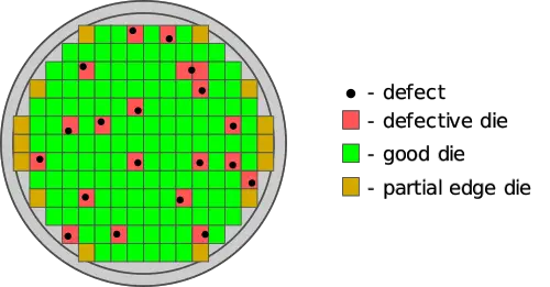
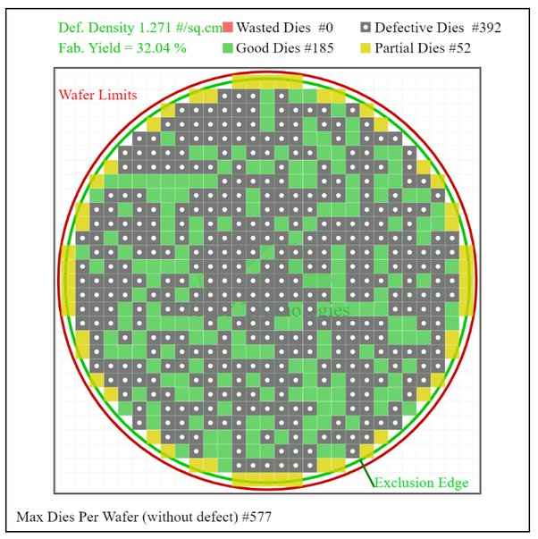
Gross die yield quantifies the number of usable chips from a semiconductor wafer, serving as a vital efficiency and quality benchmark in semiconductor manufacturing. It’s calculated by dividing the total number of functional dies by the initial quantity produced, reflecting the effectiveness of the wafer fabrication process. Software for calculating gross die per wafer is often employed to determine this metric, accurately facilitating analysis and optimization efforts.
High gross die yield indicates successful yield optimization, which is critical for producing cost-effective and high-quality integrated circuits. This metric impacts profitability and guides decisions in wafer yield and defect management, highlighting the importance of precision in semiconductor manufacturing processes.
Various factors influence gross die yield, including material quality, fabrication techniques, and equipment calibration. For instance, photolithography, etching, and deposition process variations can introduce defects that reduce yield. Additionally, the circuit design’s complexity and the precision of the manufacturing equipment play significant roles.
Employing statistical process control and cloud-based solutions can help monitor and improve these factors, leading to better yield rates. Thus, understanding and optimizing these elements are essential for wafer productivity and achieving optimal gross die yield in the semiconductor industry.
Critical Steps in Maximizing Gross Die Yield
Maximizing gross die yield within semiconductor manufacturing necessitates a focused strategy on detailed process optimization, diligent equipment calibration, and proactive defect management.
A. Process Optimization
Optimizing fabrication processes underpins yield improvement efforts. Each aspect is critical:
1. Material Selection:
The choice of materials affects the device’s functionality and reliability. It is essential to select materials that meet specific device requirements while minimizing defects.
2. Photolithography:
The precision of this step is vital for defining accurate circuit patterns. Emerging semiconductor technologies, like extreme ultraviolet lithography (EUV), are key to creating finer patterns for advanced chips.
3. Etching:
Selective material removal with minimal adjacent area damage requires a careful balance of chemical reactivity and physical bombardment. Techniques like plasma etching are central to this balance.
4. Deposition Processes:
Achieving layer uniformity is crucial. Methods like chemical vapor deposition (CVD) and atomic layer deposition (ALD) allow for the controlled addition of materials essential for complex structures.
5. Annealing Techniques:
Proper annealing improves material properties by repairing lattice damage and activating dopants, which are important for device performance.
B. Equipment Calibration and Maintenance
Equipment accuracy and maintenance are directly linked to yield:
1. Regular Calibration Schedules:
Calibration ensures equipment operates within precise parameters, which is important for tools like photolithography steppers.
2. Preventive Maintenance Procedures:
A proactive maintenance approach prevents potential yield-impacting issues, reducing downtime and equipment failures.
C. Defect Management
Effective defect management is critical to maintaining high yields:
1. Inspection Methods:
Employing various inspection techniques, from optical to electron microscopy, allows early detection of defects.
2. Defect Categorization:
Understanding defect origins and impacts helps prioritize efforts toward significant yield-affecting issues.
3. Defect Reduction Techniques:
Implementing cleanliness measures and refining processes based on defect analysis can significantly reduce defect occurrence.
These strategies focused on the granular aspects of semiconductor production, are essential for achieving optimal gross die yields. They address immediate yield challenges and lay the groundwork for ongoing efficiency and product quality advancements.
Yield Monitoring and Control
Introducing real-time monitoring systems into semiconductor manufacturing marks a pivotal shift toward proactive yield management. These systems provide immediate visibility into the performance of the wafer fabrication process, allowing for swift identification and correction of any deviations from expected yields. This immediate feedback loop is vital for maintaining optimal production levels, pinpointing inefficiencies, minimizing waste, and boosting overall productivity and gross die yield.
Statistical process control (SPC) methods are key to continuous improvement. By applying statistical techniques to analyze yield data, manufacturers can detect trends and anomalies that may suggest process variances or potential issues before they escalate into larger problems.
This approach facilitates early intervention, reducing the frequency of defects and promoting yield optimization efforts. Cloud-based solutions further improve SPC’s capabilities, enabling the aggregation and analysis of vast data across different production sites. This integration fosters a data-driven culture prioritizing precision, efficiency, and innovation to achieve superior semiconductor manufacturing outcomes.
Emerging Technologies and Best Practices
In semiconductor manufacturing, emerging technologies are reshaping the industry’s approach to increasing gross die yield. Extreme ultraviolet lithography (EUV) enables more precise patterning on silicon wafers, which is essential for producing smaller, more complex integrated circuits.
Similarly, advancements in metrology tools provide accurate measurements at the nanometer scale, ensuring that fabrication processes adhere to strict quality standards. The transition towards 3D NAND technology represents another leap forward. It offers higher storage densities and improved efficiency, directly contributing to yield improvements.
Leading companies integrate several best practices to maximize gross die yield. Adopting statistical process control (SPC) is critical, allowing firms to monitor process variability and make necessary adjustments in real-time.
Cloud-based solutions facilitate the aggregation and analysis of manufacturing data across global operations, decision-making, and defect management. Continuous training programs ensure that personnel remain proficient in technological advancements, maintaining the workforce’s ability to address evolving manufacturing challenges. Together, these strategies and technologies can optimize semiconductor production processes.
Future Trends in Gross Die Yield Optimization
The future of Gross Die Yield optimization in semiconductor manufacturing is set to be reshaped by integrating artificial intelligence (AI) and machine learning (ML) technologies. These advancements are expected to significantly improve the precision and efficiency of wafer fabrication, leading to higher yield rates.
Technological progress is anticipated in the introduction of advanced defect management systems, utilizing AI and ML to detect and address potential defects earlier in manufacturing. This early detection allows corrective actions to be taken sooner, reducing defect rates and boosting Gross Die Yield. AI-based statistical process control will enable finer adjustments to fabrication processes, maintaining optimal conditions for maximum yield.
AI and ML’s contribution to yield optimization will extend to wafer yield management and fabrication. AI algorithms are expected to identify previously unnoticed patterns and insights by analyzing extensive datasets from manufacturing operations. These discoveries can optimize wafer exposure techniques and improve mask field utilization, directly influencing Gross Die Yield. Adopting cloud-based solutions integrated with AI offers a scalable way to apply these sophisticated analytical tools across manufacturing sites, promoting a unified approach to yield optimization.
How yieldWerx™ Can Help in Boosting Gross Die Yield
yieldWerx provides semiconductor manufacturers with a customizable solution to optimize gross die yield on wafers. Engineers can customize yield calculations to specific operational needs and product requirements through its Gross Die Per Wafer Calculator module. This ensures accurate yield metrics reflecting factory operations and product characteristics without custom scripting.
With yieldWerx, manufacturers can adjust for multi-product wafers, factor in retest operations and redundancy schemes, and optimize processes for increased efficiency and profitability in semiconductor manufacturing.
Conclusion
To boost gross die yield, semiconductor manufacturers must focus on precise defect management, statistical process control, and applying artificial intelligence and machine learning to refine wafer fabrication. Embracing these practices and integrating cloud-based solutions for data analysis and scalability is essential.
For those in the semiconductor industry looking to improve their gross die yield, yieldWerx offers specialized solutions through innovative technology.
Frequently Asked Questions (FAQs)
1. What distinguishes gross die yield from other yield metrics?
Gross die yield measures explicitly the ratio of usable chips to the total number of chips produced on a wafer, focusing on the initial production effectiveness before further testing and assembly. In contrast, other yield metrics may consider additional stages of the manufacturing process or specific types of defects.
2. How does process optimization influence gross die yield?
Process optimization improves gross die yield by boosting the efficiency and accuracy of semiconductor fabrication processes, such as photolithography, etching, and deposition. This reduces the incidence of defects and increases the number of usable chips produced.
3. What importance does defect management have in yield maximization?
Defect management is crucial for identifying, analyzing, and mitigating the sources of defects in the manufacturing process, directly contributing to higher gross die yields by ensuring more chips meet quality standards.
4. How frequently should equipment be calibrated to ensure optimal performance?
Equipment should be calibrated regularly according to manufacturer recommendations and based on the operational environment and usage patterns to maintain precision in the manufacturing process and support optimal yield outcomes.
5. Which cloud-based solution is effective for yield maximization?
Cloud-based solutions like yieldWerx offer specialized tools for analyzing manufacturing data, enabling semiconductor manufacturers to identify yield detractors and implement targeted improvements, thereby maximizing yield.
6. Does a larger die size impact the overall wafer yield positively or negatively?
A larger die size generally decreases the overall wafer yield because fewer dies can fit on a wafer, and the probability of defects affecting each die increases, potentially leading to lower yield rates.
7. What factors influence the yield of a wafer?
The yield of a wafer is affected by various factors, including the precision of fabrication processes, the quality of raw materials, equipment calibration, defect management strategies, and the complexity of the chip design.
8. How is gross die per wafer calculated?
The gross die per wafer is calculated by dividing the total area of the wafer by the area of a single die, adjusted for the edge exclusion area where no dies can be placed, providing an estimate of the maximum number of dies that can be produced on a wafer.


