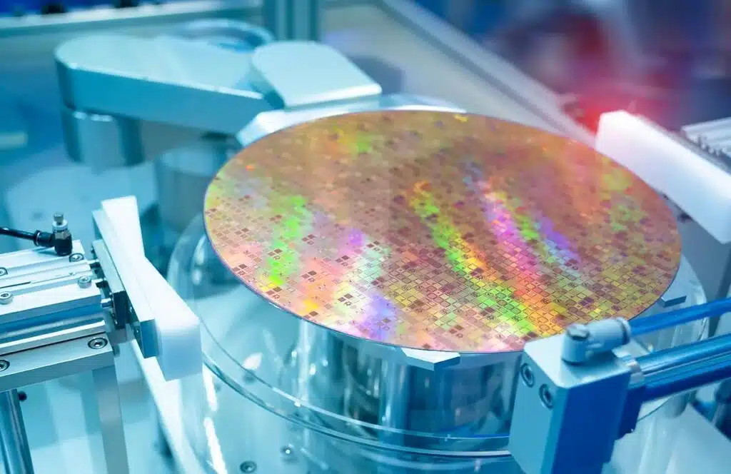
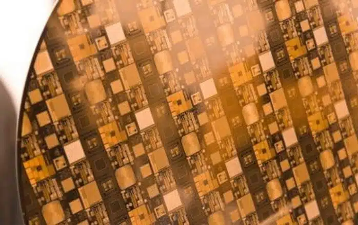
Wafer testing is a key step in semiconductor manufacturing, verifying the high standards expected in today’s technology. This process checks the quality and performance of wafers, the thin slices of silicon used to make electronic circuits. It’s a complex task that demands careful attention, as even minor errors can have big impacts.
Large automated machines, known as probe stations, are equipped with sophisticated test equipment and probe cards designed to make contact with individual dies on a wafer. These stations perform a series of tests to assess the dies’ functionality and adherence to specifications. Wafer test analysis involves a deeper examination of the test results to understand the underlying causes of defects or performance issues. It’s about turning data into insights, ensuring each wafer meets current standards and contributes to the continual enhancement of semiconductor manufacturing.
In this article, we will explore the basics of wafer testing and discuss the best practices that ensure each wafer is up to the task, which is essential for anyone working in the semiconductor industry, from engineers to quality control experts.
Wafer Manufacturing Process
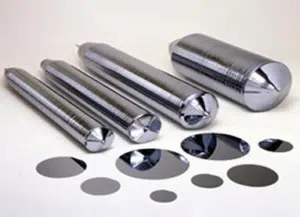
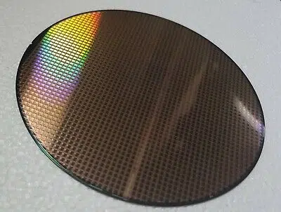
he manufacturing of wafers starts with silicon, second only to oxygen in abundance on Earth. Silica sand is initially heated beyond its melting point. A silicon seed crystal is then inserted into this molten sand using the Czochralski method, resulting in the formation of a solid silicon ingot. This ingot is sliced into thin wafers with a diamond saw, guaranteeing optimal thinness and flatness. Post-slicing, each wafer undergoes etching and polishing to achieve a surface that is as smooth and uniform as possible which is critical for precision processing and testing.
Selecting the Right Wafer
Choosing the right wafer for a specific task is a crucial decision. Different applications need wafers with different properties. When selecting a wafer, consider factors like what material the wafer is made of and its specific features. These details are important because they affect how well the wafer will work in a particular application.
Steps of Wafer Testing
Here are the steps of wafer testing, encompassing a series of detailed and specialized procedures vital to confirming the quality and functionality of semiconductor devices.
Visual Inspection:
Visual inspection is the first step, where each wafer is closely examined for visible flaws or damage. Technicians look for cracks, scratches, or any irregularities on the surface. This step is crucial as physical defects will limit the performance of the wafer during wafer testing.
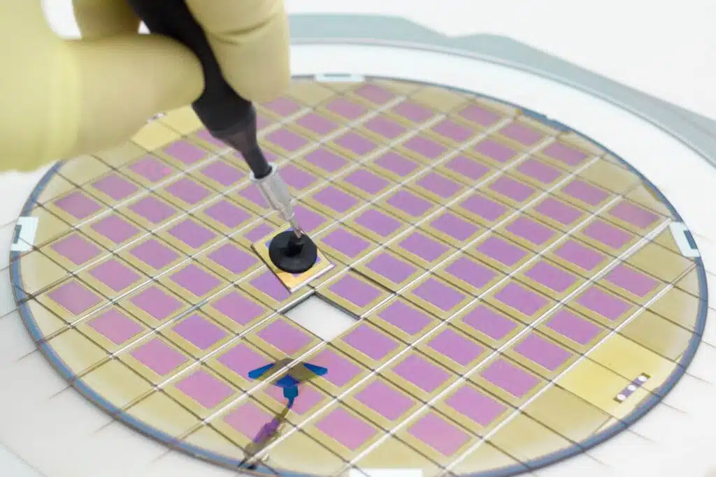
Wafer Probing:
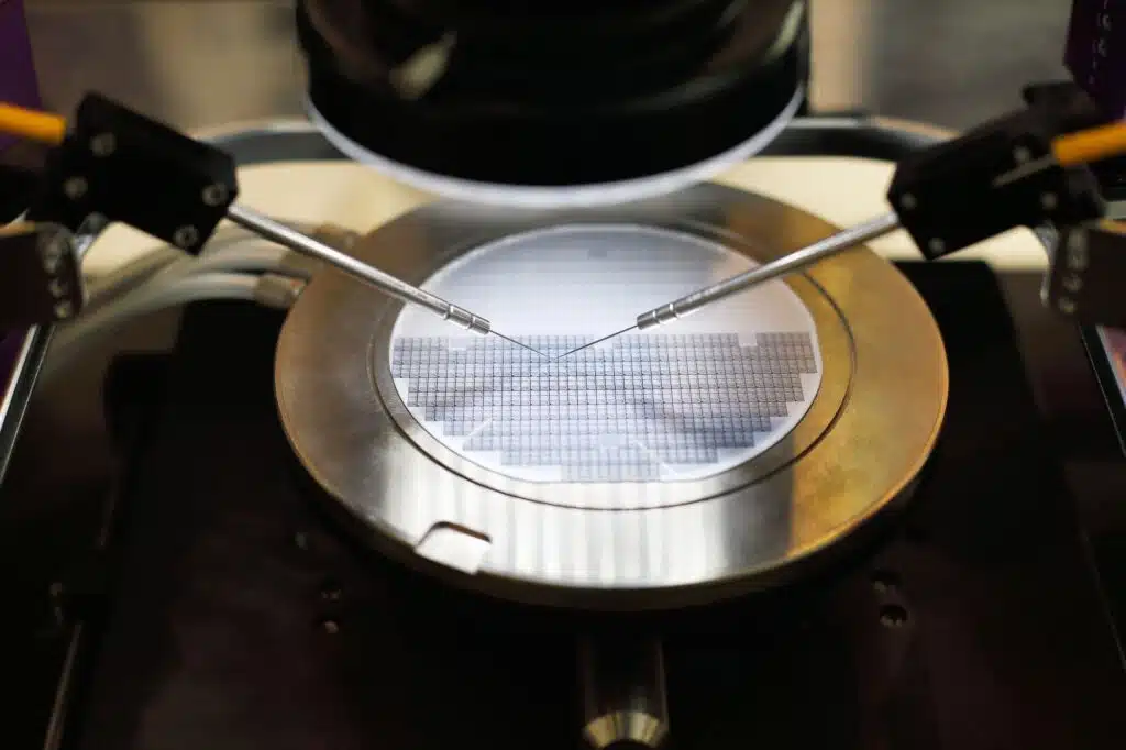
In this stage, a probe card is used. This equipment tests the electrical properties of the circuits on the wafer using chip probe techniques. Each tiny area on the wafer (known as a die) is tested to make sure it conducts electricity properly. This step is critical for finding any electrical issues early on.
Die Test:
After probing, each individual die on the wafer undergoes a more detailed test. This die test checks for functional defects in each circuit. It’s crucial to guarantee that part of the wafer works as it should.
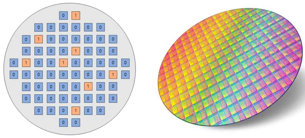
Binning and Dicing:
Based on the test results, individual dies on the wafer are sorted or “binned” according to their performance. Dies that meet the required specifications are classified for further processing, while those that don’t are either retested, if possible, or discarded. This sorting can also categorize dies based on performance levels for different product grades. Once the dies have been tested and sorted, the wafer is cut, or “diced,” into individual dies. This is typically done with a precision saw or laser cutting technique.
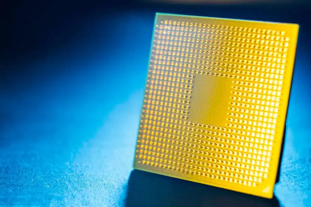
Chip Packaging and Testing:
The functional dies are then packaged, where each die is placed in a protective casing with external contacts added. This step involves several sub-steps, including die attachment, wire bonding (or flip-chip bonding), and encapsulation. The package protects the die and allows it to be mounted on a circuit board after packaging, the chips undergo final testing to ensure they function correctly within their intended operating environments. This step tests the integrated circuit within its package for functionality, performance, and compliance with the specified standards.
Types of Test Wafers
In the field of semiconductor testing, various types of test wafers are employed to meet specific manufacturing and quality assurance needs, utilizing chip probes and other techniques.
Monitor Wafers:
These wafers are employed to check the overall health of the semiconductor fabrication process. They undergo the same manufacturing steps as actual product wafers. Analyzing these monitor wafers provides technicians with essential insights into the performance and potential issues in the manufacturing process.
Dummy Wafers:
Made to resemble real wafers without actual chip structures, dummy wafers serve as placeholders in the production line. Their primary function is to ensure equipment calibration and readiness when actual wafers are not being processed.
Defect Wafers:
Defect wafers are intentionally created with known defects, such as pattern irregularities or material impurities. They allow manufacturers to study how defects impact wafer performance. This understanding is vital for detecting and correcting problems early in the manufacturing process.
Short Loop Wafers:
Although less common, short-loop wafers are essential in specialized testing scenarios. They offer critical insights into semiconductor performance under specific conditions, such as testing for specific environmental conditions or stress levels, aiding in the optimization of the manufacturing process for improved product quality.
Each type of test wafer, be it a monitor, dummy, defect, or short loop, plays a distinct role in maintaining high standards in semiconductor testing. These wafers, along with the use of wafer probers and comprehensive chip and die tests, contribute significantly to the production of reliable and high-quality semiconductor products.
Key Practices in Wafer Test Analysis
In wafer test analysis, a blend of precision and attention to detail is vital. From selecting the right materials to designing wafers that accurately replicate production models, every step is crucial. Employing various testing methods like electrical testing for device functionality, Lot Genealogy in Wafer Final Test. Scanning Electron Microscopy (SEM) provides detailed imaging of wafer surfaces, and Focused Ion Beam (FIB) techniques are used for precise material manipulation and analysis.
Ensuring quality control through routine inspections and regular equipment calibration is key to reliable results; these practices ensure the testing equipment’s accuracy and consistency, which is fundamental for reliable test results. Tools such as wafer probers and probe stations accurately assess each wafer’s performance. Furthermore, analyzing data effectively helps pinpoint issues and trends, while troubleshooting skills are necessary to resolve any problems. These practices are the foundation of proficient wafer test analysis, contributing significantly to the high standards of semiconductor testing.
Data Collection and Precision Measurement:
Data collection is the first step in wafer testing analysis. It’s important to gather accurate and comprehensive data from each wafer test. This includes electrical measurements, defect analysis, and more. Using software like yieldWerxTM streamlines the collection and organization of data from wafer probers and chip testers, automating anomaly and trend detection to simplify analysis. Precision in these measurements is fundamental, as they form the basis for further analysis and decision-making.
Advanced Data Interpretation:
The data collected from wafer tests is extensive and complex. Advanced data interpretation methods are essential to extract meaningful insights from this data. This is where sophisticated software like yieldWerx comes into play, offering powerful tools for data analysis, reporting and interpretation, turning raw data into actionable intelligence.
Commonality Analysis offers a structured approach to identifying patterns and correlations in failure data. This technique involves examining the test results from various wafers to spot common failure trends or recurrent issues. By pinpointing these commonalities, engineers can trace back to the potential root causes of failures, whether they stem from specific steps in the manufacturing process or particular batches of materials.
Process Control and Optimization:
Effective wafer test analysis isn’t just about detecting problems; it’s also about ensuring the manufacturing process is controlled and optimized. This involves regular monitoring and fine-tuning of the process parameters to maintain high standards of quality and efficiency. Strategies like Statistical Process Control (SPC) are integral in this aspect, providing a systematic approach to process monitoring.
Reliability Testing:
In semiconductor testing, ensuring the long-term reliability of the devices is paramount. Reliability testing involves subjecting the wafers to various stress conditions and predicting their lifespan and performance under different scenarios. This practice helps in guaranteeing that the semiconductors will perform reliably in real-world conditions.
Integration with Manufacturing Workflow:
Wafer test analysis should be integrated with the overall semiconductor manufacturing workflow. This ensures that the insights gained from the analysis can be promptly and effectively implemented, leading to immediate improvements in the manufacturing process. The integration also helps in maintaining a continuous flow of information, enabling a proactive approach to quality control.
Case Studies
In semiconductor manufacturing, case studies demonstrate the impact of best practices in wafer testing.
NI Cuts Costs with Advanced Automated Test Equipment
One notable example comes from NI (National Instruments), recently acquired by Emerson, where advanced semiconductor technology and processing research is conducted, including next-generation logic devices and 3D stacked integrated control (IC) system integration. They faced challenges with wafer/chip processing in their R&D environment, particularly with defects occurring over the entire process flow, leading to a significant drop in functional-device yield.
To address this, they implemented an in-fab semiconductor automated test equipment (ATE) setup capable of handling 24/7 test operations. This setup significantly reduced R&D project deliverable time and decreased overall costs. The initial tester version combined NI PXI SMUs with a digital multimeter, LCR meter, and third-party low-leakage switch matrix. They developed a custom probe card and linked all wafer-probing components to a PXI instrumentation rack.
The use of LabVIEW parametric test routines on the in-fab ATE using PXI modular instruments allowed for fully automated, unattended wafer tests at several stages of the process flow. This resulted in impressive improvements in testing efficiency and effectiveness, demonstrating the importance of integrating advanced testing methods and equipment in semiconductor research and development.
Improving Semiconductor Inspection with Nikon Metrology’s Advanced Optical Technology
Another case study involves Nikon Metrology Inc., which illustrates the application of advanced optical technology in the semiconductor industry. Nikon’s camera and optics technology has been utilized for various applied research tasks, including inspecting and quality-controlling semiconductor wafers. While specific details of their semiconductor-related case studies weren’t available, the company’s expertise in optics and imaging contributes significantly to the precision and efficiency of semiconductor inspection processes. This suggests the critical role of high-quality imaging and microscopic technology in enhancing the accuracy of wafer testing and inspection.
Future Trends in Wafer Testing

The future of wafer testing in the semiconductor sector is poised for innovative developments, notably through nanotechnology, for more accurate 3D integration testing for improved chip functionality with reduced size.
Artificial intelligence (AI) is also becoming increasingly important in wafer testing. AI can analyze data from tests much faster and more accurately than humans. It can quickly identify patterns and anomalies that might indicate a problem with the wafer. As AI technology advances, its applications in wafer testing will become more sophisticated, leading to faster and more reliable testing processes.
How can YieldWerx Help with Wafer Testing & Analysis?
yieldWerx provides advanced solutions for wafer testing and analysis, enabling semiconductor manufacturers to improve product quality and efficiency. The platform offers detailed insights and control over the testing process, ensuring optimal performance and yield.
Wafer Prober Control Module
The Wafer Prober Control module optimizes the integration of prober and tester equipment, facilitating effortless operation during wafer testing. It improves test accuracy and efficiency, reducing manual intervention and improving throughput.
Cross Work Center Correlation
This module allows root cause analysis, data comparison, and correlation across different manufacturing sites and equipment. It identifies variations and potential issues, ensuring consistency and quality throughout the production process.
Wafer Lot Disposition Control Tool
The Wafer Lot Disposition Control tool offers comprehensive management of wafer lot releases, retests, and holds. It provides automated decision-making capabilities based on test data, improving operational efficiency and reducing time to market.
Concluding Thoughts
The importance of best practices in wafer testing cannot be overstated for the semiconductor industry. High-quality wafer testing ensures the reliability and performance of semiconductor devices, which are integral to almost every modern technology. Additionally, wafer test analysis, a critical component of this process, involves evaluation and data interpretation to ensure each semiconductor meets the highest standards of quality and functionality, further solidifying the industry’s commitment to excellence and innovation.
By continuously enhancing wafer testing practices and embracing technological innovations, and cloud-based testing solutions like yieldWerx, the semiconductor industry is well-positioned to keep pace with the rapid technological advancements shaping various sectors. It offers a flexible, end-to-end yield management platform that perfectly adapts to the unique demands.
Schedule your demo today and see why we’re the semiconductor industry’s top choice for precision, efficiency, and innovation.